
An Overview
In 2026, with the rapid change in technology, data is the new air! We breathe it through AI models, 8k-4k videos, and massive Cloud networks. However, our physical storage has a secret limit. Every time we write or erase data to a flash memory, it wears out. This process can cause uneven wear, where certain memory blocks degrade faster than others, leading to early failure of those blocks.
As technology updates faster than ever, the newer memory drives faster and holds more data but has shorter lifespans. These limitations are due to the physical properties of NAND flash memory cells, which are prone to flash wear from repeated write and erase cycles. Solid state drives (SSDs) and other flash memory devices rely on wear leveling technology to prevent uneven wear and premature failure. The SSD controller manages wear leveling and tracks write cycles to ensure data writes are evenly distributed across all physical memory blocks. In this situation, wear leveling is not just a background task—it is the primary guardian of our digital memories, and without it, our storage system would fail much sooner than expected. Wear leveling is a technology used in flash memory devices to evenly distribute data writes across all physical memory blocks, preventing premature failure.
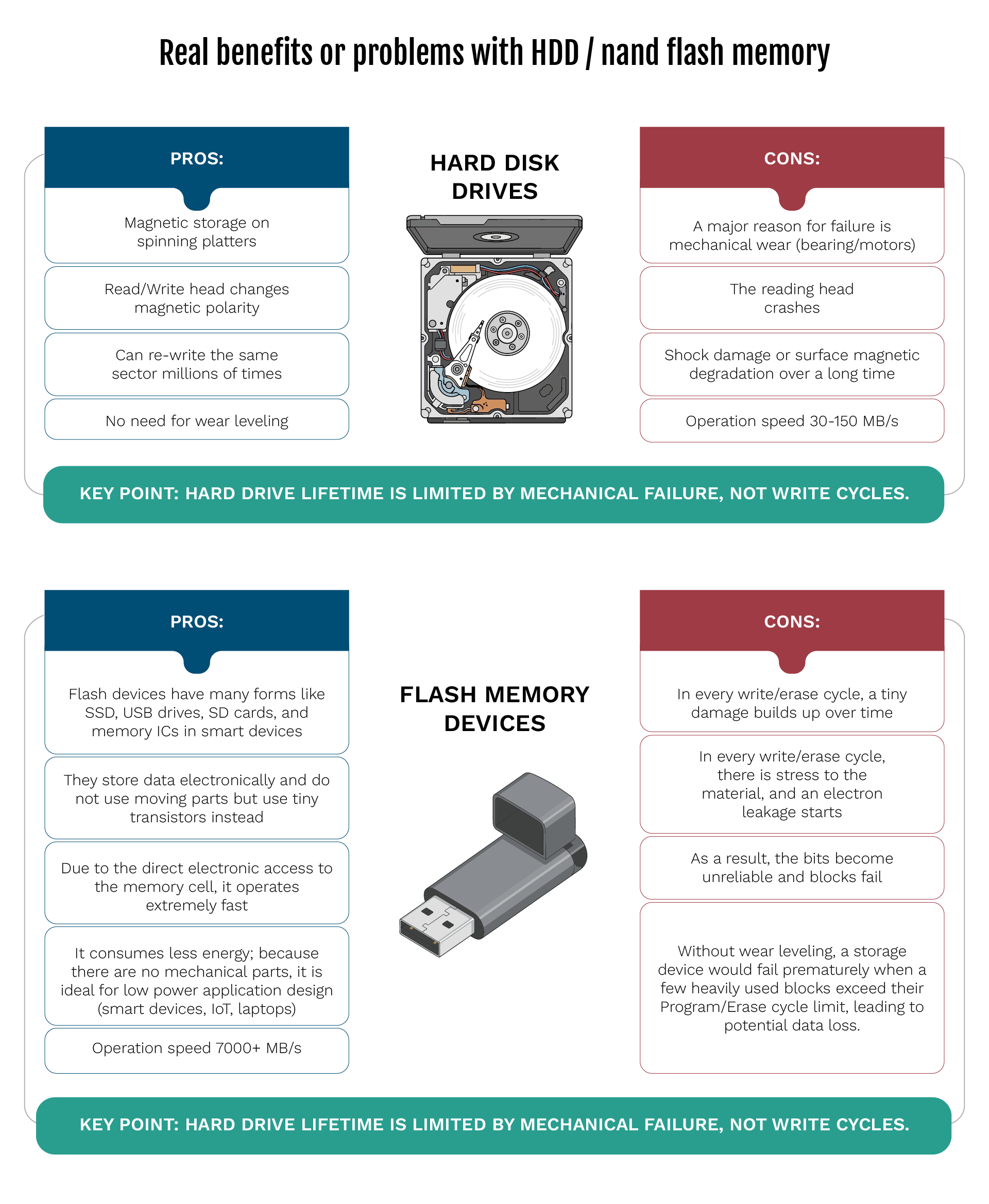
Real benefits or problems with HDD / nand flash memory
The global scenario is rapidly changing, and devices need to compute instructions lightning fast, while also being smaller and more compact. We need to create better storage devices operating at higher speeds and in compact sizes.
The various kinds of storage devices that we have today are:
File systems, such as JFFS2, YAFFS, and ZFS, play a significant role in how data is written and managed on flash memory devices, directly impacting wear leveling and device longevity. Wear leveling groups within a flash storage device help segment and manage data based on importance and reliability needs, improving efficiency and data integrity. Wear leveling enhances overall data integrity by preventing the premature exhaustion of flash cells.
Reasons Why Flash Memory Wears Out
- In a flash drive, data is stored in NAND flash memory cells in the form of electrons within a tiny transistor. Each of these transistors has an oxide layer. Data is represented as an electrical charge in the floating gate of each memory cell, and the integrity of this charge is critical for data retention and the longevity of NAND flash memory.
- With each erase/write, or in technical terms the P/E cycle (Program/Erase cycle), on NAND flash memory, the following changes take place:
- The memory cells wear out because of electron tunnelling through an insulating oxide layer. This process stresses the material barrier due to the use of high voltage.
- Erase operations are particularly stressful for NAND flash memory cells and contribute significantly to flash wear.
- Over time, it degrades the oxide layer.
- It can no longer hold charge reliably, and the block fails.
- Eventually the cell becomes unstable (bit flips) and becomes unusable.
| Program/Erase (P/E) Cycle Limits
Each flash cell has limited cycles: |
|
| Type | Typical Endurance (Cycles) |
| SLC – Single level cell(1bit/cell) | ~100,000 |
| MLC – Multi level cell (2bit/cell) | ~10,000 |
| TLC – Triple level cell (3bit/cell) | ~3,000 |
| QLC – Quad level cell (4bit/cell) | ~1,000 |
What Is Dynamic Wear Leveling and How Does It Work?
Flash memory has critical constraints, and we cannot overwrite data directly.
Instead:
- Data must be erased (entire block level)
- Then reprogrammed/write (in page level)
Wear-leveling is a flash memory management algorithm. Using this process, the data write/erase cycle distributes evenly across all flash blocks. So, no single block gets overused.
A simple visual representation of wear-levelling:
- Without wear-levelling
Block A: ███▒▒▒▒▒▒▒ 30%
Block B: ███████▒▒▒ 70%
Block C: █▒▒▒▒▒▒▒▒▒ 10%
Block D: ████▒▒▒▒▒▒ 40%
Block B is used repeatedly. It fails early, while others are still healthy. - With wear-levelling
Block A: ███▒▒▒▒▒▒▒ 30%
Block B: ███▒▒▒▒▒▒▒ 30%
Block C: ███▒▒▒▒▒▒▒ 30%
Block D: ███▒▒▒▒▒▒▒ 30%
The incoming data writes are distributed evenly. All blocks age at the same rate.
Here is how it works:
- Identifies “COLD” and “HOT” blocks: The wear-levelling algorithm monitors the erase count of each block. The “HOT” blocks are those that are frequently written to, while the “COLD” blocks are rarely updated.
- Types of Wear-leveling
- Dynamic Wear-levelling: In this mode, the incoming data is written into the available free space. The data write operation is performed on the block which has the least number of erased counts. As an example, the OS data or any system files that have not been touched, and which were saved a long time ago.
- Static Wear-Levelling: In this mode, the process calculates the erased cycle of all blocks COLD and HOT. So, if a new data block needs to be written, and the available block’s erase count is high, then the old data (rarely modified or used) is moved to here and the new data is written into the recently cleaned less erased count block. This process is followed to maintain the P/E cycle for long term use of flash memory.
- Memory Mapping: During wear-leveling, the system keeps changing how the physical memory blocks are mapped to the logical addresses that the software uses. This means that the software always sees the same logical address, even if the data is moved to a different physical location. Due to this abstraction, data can be shifted around inside the memory without the operating system picking up on it.
Do Wear Leveling Algorithms Make Flash Memories Immortal?
Wear-leveling does not make flash memory immortal. It simply helps it last longer. It works by spreading the wear across all memory blocks so that no single block wears out too quickly. This slows down the aging process and makes the device more reliable over time. However, it cannot fix physical damage, repair worn-out oxide layers, or remove the built-in limits of the hardware. Flash memory still has a fixed number of P/E cycles. In the end, wear-leveling only ensures that all blocks wear out evenly; it does not mean that they last forever.
Know More: Consumer Electronics Design And Engineering Services
Frequently Asked Questions
- Does wear-levelling improve SSD/Flash drive performance?
Its primary purpose is to extend the lifespan of flash memory. While it can help maintain consistent performance over time. It is not designed to make the SSD/Flash memory faster. - Does Wear Levelling slow down SSD/Flash drives?
No. Modern controllers handle this instantly. This process usually runs when the computer or system is idle. - Is wear-levelling used only in SSDs?
No. Wear levelling is used in many flash-based storage devices, including USB flash drives, SD cards, eMMC, UFS, EEPROM, and embedded systems that use NAND flash memory - Can wear levelling prevent flash memory from failing?
No, wear-levelling can’t stop flash memory from wearing out. It only delays failure by ensuring that all memory blocks age at the same time and rate. - What happens when a cell dies?
The drive marks it as a “bad block” and stops using it. The data is safely moved to a fresh spare cell. - What is the difference between wear-levelling and garbage collection?
Wear-levelling balances write operations across memory blocks. While garbage collection removes invalid data and frees space for future writes. Both processes work together to improve SSD efficiency and reliability. - Should we “defrag” the SSD?
Never. Defragging writes massive amounts of useless data. It wears out the memory drive faster and undermines wear levelling. - Do users need to enable wear-levelling?
No. Wear-levelling is built into the firmware of modern SSDs and flash memory storage devices. It operates automatically without any user intervention. - Can wear-levelling be implemented in embedded systems?
Yes. In embedded systems, developers can implement wear levelling in software. They store data in different memory locations rather than writing to the same location every time. They also keep track of block usage and identify the latest valid copy of the data - How can we increase the lifespan of SSD/Flash memory beyond wear levelling?
- Avoid unnecessary write operations.
- Keep sufficient free storage space.
- Update the SSD or flash memory firmware when the manufacturer recommends it.
- Use the SSD/flash memory within its recommended operating conditions.