


AI-driven chip design means two things: building processors specifically for Artificial Intelligence (AI) workloads and using AI tools inside semiconductor development to improve work such as design optimization and verification. AI is reshaping not just the demand for silicon, but the very process of creating it. The real story goes beyond any single market forecast. It sits at the intersection of custom computing, advanced packaging, design complexity, verification of bottlenecks, and AI-powered engineering tools.
For semiconductor engineers, chip designers, technology industry professionals, and other stakeholders tracking how AI is changing chip development, separating these two meanings makes the shift easier to understand. This article looks at the push toward specialized and custom silicon, the growing complexity of chip system design, where verification slows development, and where AI can realistically help across the design flow. Those changes matter because AI is changing both what chips need to do and how teams have to build them, raising the need for more specialized silicon and more efficient engineering methods at the same time.
A demand shock from AI infrastructure in data center servers
According to the World Semiconductor Trade Statistics, global semiconductor sales reached $795.6 billion in 2025, up 26.2% from 2024. Logic and memory led the charge, driven by data-center infrastructure, AI accelerators, and high-bandwidth memory. That represents a broader and more dependable demand signal than any narrow forecast for the “AI chip market”, a category that research firms tend to define quite differently from one another.
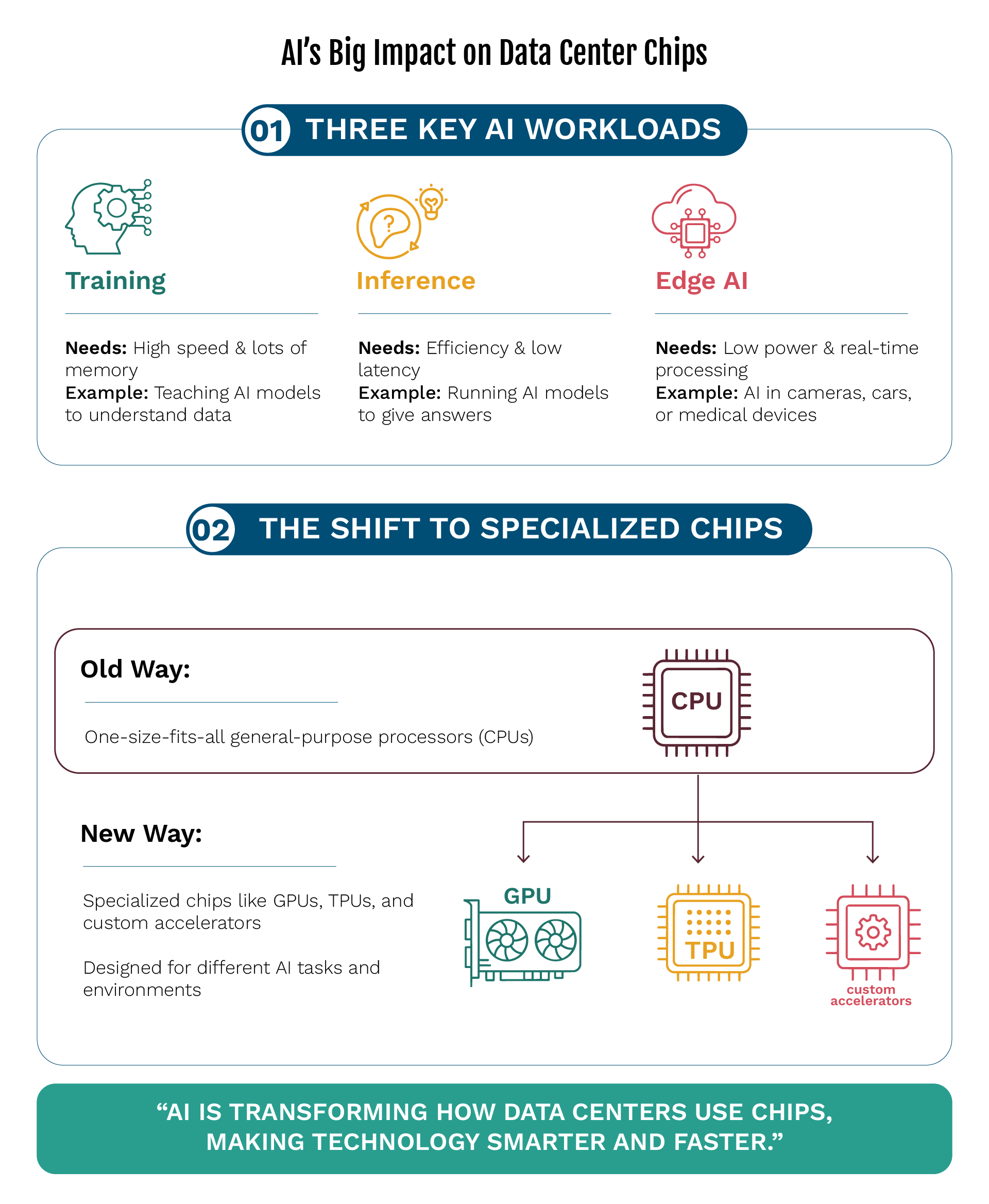
This demand is not concentrated on a single type of processor. Training large models calls for massive parallel compute and rapid memory access, and that shift is accelerating as Moore’s law slows, and chip-design demands face increasing complexity. Inference brings a different set of pressures altogether: cost per query, latency, power consumption, and the ability to serve models reliably at scale. Move to the edge, and the priorities shift once again. A camera, a vehicle, a medical device, or an industrial controller may need real-time inference within tight power and thermal limits, often without sending sensitive or time-critical data to the cloud.
Such a wide spread of workloads is pulling the market away from a one-size-fits-all mindset. GPUs remain central to AI computing, but companies are increasingly turning to application-specific accelerators, custom CPUs, networking silicon, DPUs, and domain-specific accelerators used across machine learning, genomics, robotics, and other domains for various applications in deep learning infrastructure and edge systems. Google’s TPU is a well-known example built to accelerate deep neural networks inference in large-scale ai infrastructure. This is not a story about general-purpose silicon being replaced by any single general-purpose processor. It is a story about the compute landscape becoming significantly varied and specialized.
Custom silicon and domain specific accelerators have moved into the mainstream
The most compelling proof comes straight from the cloud giants themselves. AWS describes Trainium as a purpose-built effort in custom silicon that spans chip architecture design and IP integration, designed as part of a tightly integrated stack that brings together data center servers, networking, software, and cloud services. Google has kept pushing its Tensor Processing Unit family forward to serve both its own models and its cloud customers. Microsoft has launched the Maia accelerator for Azure AI workloads, while Meta has grown its in-house MTIA family to support recommendation and generative AI infrastructure. The logic behind this trend is simple. At hyperscale, even small gains in utilization, memory movement, power efficiency, or cost per token can translate into enormous economic advantages. Owning more of the hardware and software stack also gives a company the freedom to shape its computer architecture around real, live workloads, where AI-optimized layouts can improve performance, deliver higher efficiency, and lower energy consumption rather than chasing some broad market average.
What is interesting is that this workload-first way of thinking is now spreading well beyond the cloud. Automotive systems, especially autonomous systems, are pushing accelerator design toward specialized hardware and integrated circuits that can handle perception, sensor fusion, and real-time decision-making. Consumer devices are gaining on-device language, imaging, and speech capabilities. Industrial and healthcare systems demand low-latency inference, long product lifespans, and in many cases much stricter safety assurance. One of the key benefits is that each application domain can adopt domain-specific acceleration based on its own mix of performance, power consumption, safety requirements, cost, and programmability.
The chips are becoming systems, not isolated dies
At the same time, the physical design problem is getting harder. Advanced process nodes deliver real gains in density and energy efficiency, but they also drive up the cost and complexity of achieving design closure, especially as Dennard scaling slows and broader technology scaling limits push the industry toward more specialized integration. TSMC kicked off volume production of its N2 nanosheet technology in 2025 and is already pushing its roadmap further through A16 and beyond. Samsung, meanwhile, is developing its own 2nm Gate-All-Around process aimed squarely at AI and high-performance-computing workloads.
What makes this even more interesting is that many leading designs are moving beyond a single chip, with integrated circuits assembled as chiplets in one package rather than built around a single monolithic die. Instead, they bring together logic, high-bandwidth memory, I/O, and specialized functions through 2.5D and 3D integration. TSMC’s CoWoS platform is a good example of this shift – it is specifically designed to place logic chiplets and HBM side by side within the same advanced package. On the standards front, the UCIe specification is working to establish an open interface for chiplet-to-chiplet communication inside a package.
All of this reshapes the core engineering challenge in a meaningful way. Power integrity, signal integrity, thermal behavior, mechanical stress, test access, and package routing can no longer be treated as separate concerns – teams must optimize the entire system, including data movement and hardware resources, rather than individual dies in isolation. A decision that looks perfectly reasonable at the RTL or block level can quietly introduce a timing problem, a heat issue, or an interconnect headache further down the line. The boundaries that once separated chip design, packaging, and system design are growing harder to see.
Verification remains the largest practical bottleneck
Design complexity is only one piece of the puzzle. Teams also need to prove that their designs hold up across a massive range of states, workloads, and operating conditions. According to the 2022 Wilson Research Group study, IC and ASIC design engineers reported spending an average of 49% of their time on verification activities alone. The 2024 study reinforced this trend, highlighting increasing verification complexity as SoCs integrate more processors, software, analog content, security features, and reliability requirements. [10, 11]
That figure goes a long way toward explaining why verification has become such a magnet for AI investment. A tool that cuts down on redundant regressions, clusters similar failures together, or helps an engineer pinpoint the root cause of a bug can deliver real-time savings without needing to be trusted with inventing the design. That makes it a far more controlled and practical starting point than jumping straight into fully autonomous RTL generation.
Why machine learning is becoming practical inside the design flow
Machine learning has been explored in EDA research for years, but three key developments are now making it significantly more practical to adopt. For starters, modern design flows produce enormous volumes of structured data – timing reports, congestion maps, coverage databases, waveforms, failure logs, and manufacturing results. On top of that, cloud and accelerated computing now make it feasible to explore multiple design alternatives simultaneously. Most importantly, today’s models can be fine-tuned on specialized engineering language and internal design knowledge, rather than depending entirely on general data scraped from the internet.
Google’s published research on reinforcement learning for chip floorplanning served as one of the earliest convincing proof points. It demonstrated that an AI agent could produce floorplans in under six hours that matched or even outperformed human-generated layouts on key metrics, and the approach was actually deployed in Google AI accelerators. [12] NVIDIA’s ChipNeMo project later showed how domain adaptation could make large language models genuinely useful for internal chip-design work, covering things like engineering assistance, code generation, and bug summarization. [13]
Since then, commercial EDA platforms have been steadily embedding AI capabilities across design-space exploration, verification, analog optimization, test, and physical verification. Generative AI is also starting to make inroads into areas like documentation search, script generation, RTL assistance, and testbench creation. The adoption is real and growing – but it is worth noting that maturity levels vary quite a bit depending on the specific task at hand.
Power efficiency constraints are as important as the opportunity
AI doesn’t eliminate the need for clean data or sound engineering judgment. Many companies simply don’t have consistent historical data across their projects. Design information is highly sensitive that restricts where models can be trained and how data can be shared between teams. Optimizing one metric can easily hurt another. Any RTL or verification content that AI generates still needs to be carefully checked against the specification, design rules, and safety requirements.
The near-term use cases that show the most promise tend to share one important characteristic: they keep the engineer firmly in control. AI explores options, prioritizes tasks, makes predictions, clusters information, and surfaces explanations. The engineer defines the objective, reviews the output, and stays accountable for sign-off. That might sound less exciting than the idea of a fully autonomous chip designer, but it is far more relevant to how semiconductor teams actually operate today.
The market shift in one sentence
AI is increasing the need for specialized silicon while semiconductor teams need better ways to manage the complexity of designing it.
Next in the series: Where AI Is Actually Working Across the Chip Design Lifecycle
Frequently Asked Questions
1. What does AI-driven chip design mean?
AI-driven chip design covers two closely related trends. The first involves designing specialized processors built for AI workloads such as training, inference, computer vision, and edge intelligence. The second involves applying AI tools within semiconductor engineering to support tasks like floorplanning, design optimization, verification, failure analysis, and code assistance.
2. Why are companies developing custom chips for AI?
Companies build custom AI chips to achieve better performance, power efficiency, lower latency, and reduced costs for specific workloads. At high deployment volumes, even modest gains in memory movement, infrastructure utilization, or cost per inference can translate into substantial operational savings. Custom silicon also makes it easier to integrate hardware, software, networking, and cloud infrastructure more tightly.
3. How is AI currently used in semiconductor design?
AI is currently applied across a range of tasks including exploring design alternatives, optimizing power, performance, and area, prioritizing verification tests, identifying coverage gaps, grouping related failures, generating scripts, and assisting with RTL and testbench development. The most useful applications work alongside engineers rather than replacing them, and all outputs still require thorough validation and engineering review.
4. Why is verification a major focus for AI adoption?
Verification accounts for a large portion of semiconductor development effort because teams need to test complex designs across a wide range of operating conditions, software states, interfaces, and failure scenarios. AI can help by cutting down on redundant regressions, grouping related failures together, highlighting coverage gaps, and steering engineers toward the most relevant issues quickly.
Sources and further reading
1. Global Semiconductor Market grows 26% in 2025 to $796B — World Semiconductor Trade Statistics. Full-year 2025 sales and demand drivers.
2. AWS Trainium — Amazon Web Services. Purpose-built AI silicon and full-stack positioning.
3. Ironwood: The first Google TPU for the age of inference — Google. Google’s seventh-generation TPU announcement.
4. Microsoft Ignite 2023: AI transformation and the technology driving change — Microsoft. Introduction of Azure Maia and Cobalt.
5. Our next-generation Meta Training and Inference Accelerator — Meta. Public description of the MTIA family.
6. TSMC 2025 Annual Report — Business Activities — TSMC. N2 volume production and process roadmap.
7. Samsung Electronics Announces First Quarter 2025 Results — Samsung Electronics. 2nm GAA work and AI/HPC applications.
8. CoWoS — TSMC 3DFabric. Integration of logic chiplets and HBM.
9. About UCIe — UCIe Consortium. Open chiplet interconnect specification.
10. 2022 Wilson Research Group Functional Verification Study — Part 8 — Siemens EDA. Time spent by IC/ASIC design engineers on verification.
11. 2024 Wilson Research Group IC/ASIC Functional Verification Trend Report — Siemens EDA. Current verification-complexity trends.
12. A graph placement methodology for fast chip design — Nature. Peer-reviewed reinforcement-learning floorplanning research.
13. ChipNeMo: Domain-Adapted LLMs for Chip Design — NVIDIA Research. Domain adaptation for industrial chip-design language models.
14. India has emerged as a global hub for semiconductor design and R&D — Press Information Bureau, Government of India. Estimate of India’s share of the global chip-design workforce.