

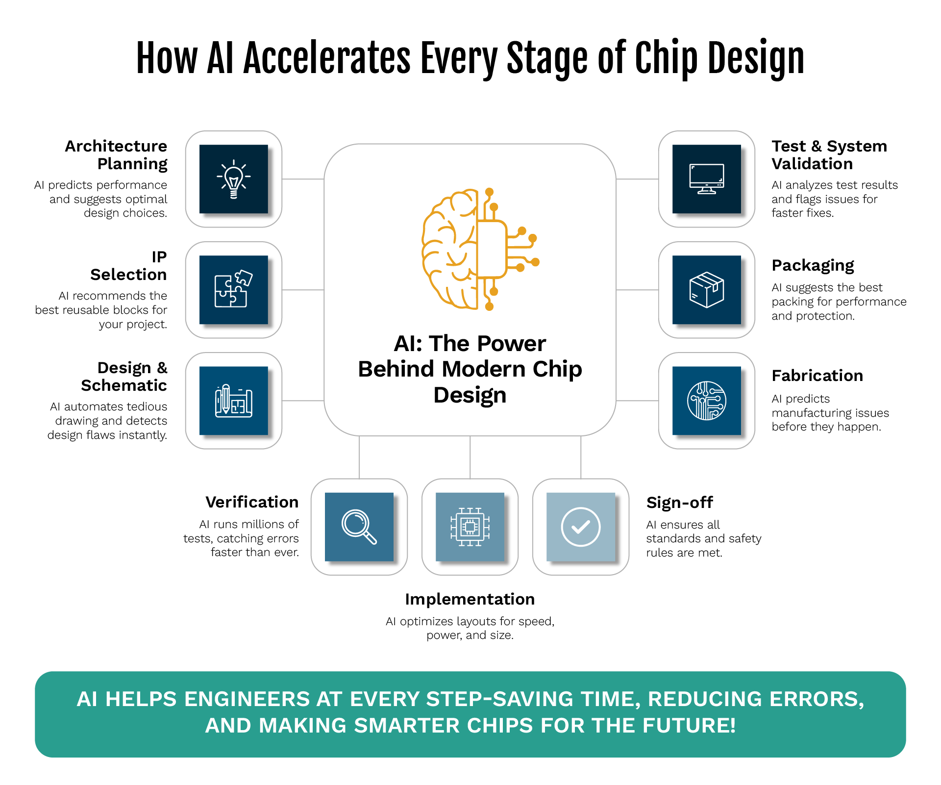
AI-enabled chip development is impacted by many parts of the semiconductor ecosystem, which underpins AI, automotive, and consumer electronics. EDA vendors, foundries, packaging providers, cloud companies, and specialist manufacturers are adding AI to selected workflows while continuing to rely on established design, validation, and manufacturing processes.
A chip design does not move from an idea to silicon through a single software platform. It moves through multiple layers of the semiconductor industry, from architecture, IP, verification, and implementation to sign-off, fabrication, packaging, test, and system validation. The industry is a global network of specialized, interconnected companies and suppliers, and every stage relies on data, models, and rules that come from different parts of the ecosystem.
The meaningful shift, then, is not some standalone “AI tool” arriving on its own. It is the steady incorporation of AI-assisted capabilities into certified flows, foundry platforms, and full-stack silicon programs.
The Broadening Use of AI In the Workflow by EDA Vendors
The three biggest Electronic Design Automation (EDA) vendors all publicly endorse AI capabilities spanning multiple stages of the design lifecycle, though their products, deployment models, and levels of maturity vary. Areas they share in common include optimization and analytics, generative assistance, data management, and recently announced agentic workflows. The descriptions below are based on vendor disclosures and are not intended as independent product comparisons or performance assessments.
Synopsys: Publicly Described AI Capabilities Across Design, Verification, Test, and Analogue Flows
Synopsys offers a range of specialized tools under its AI portfolio.
- DSO.ai is aimed at implementation design-space exploration
- VSO.ai handles verification-space optimization
- TSO.ai focuses on semiconductor test
- ASO.ai targets analog design optimization
The Synopsys.ai platform also incorporates generative and multi-agent capabilities that apply to certain design and verification workflows.
Each of these tools addresses a distinct set of tasks, so they should not be grouped together as a single, uniform level of automation.
Cadence: Publicly Described AI Capabilities Across Design, Verification, Systems, and Cloud Computing
Cadence covers design-space exploration through:
- Cerebrus
- Verification analytics
- Verisium
- A shared data layer through its JedAI platform
The portfolio also extends to analogue design, packaging, PCB, and system analysis. In 2026, Cadence announced additional ChipStack AI capabilities aimed at front-end design and verification.[2, 3] These are still vendor-described features, and publicly available evidence of repeatable production outcomes continues to develop.
For engineering teams, the wider takeaway is the importance of treating the die as part of a broader picture that includes package routing, memory, thermal behaviour, board design, and system software. AI-assisted workflows can help with parts of this challenge, but making decisions at the system level still depends on domain expertise and careful validation across tools and disciplines.
Siemens: Publicly Described AI Capabilities Across Verification, Custom IC, and multi-tool Workflows
Siemens covers AI applications across areas like:
- Calibre physical verification
- Solido custom-IC design and characterizatio
In March 2026, the company announced the Fuse EDA AI Agent, which is designed to orchestrate specific multi-tool workflows for semiconductor and PCB development. As with other recently announced agentic systems, how useful it proves in practice will depend on how it is deployed, what data it can access, how tools are configured, and how customers validate it.
For users, several considerations remain central:
- data security
- access control
- model selection
- traceability
- the ability to verify outputs
These factors carry particular weight when design IP, process information, and failure data are part of the picture.
Foundries Are Becoming Design and Packaging Ecosystems in the Semiconductor Industry
At leading process nodes, the relationship between a customer and a foundry goes well beyond simply manufacturing wafers. Customers now expect access to process design kits, qualified EDA tools, silicon-proven IP, reference flows, packaging options, and dedicated design support.
AI is making its way into this broader ecosystem through applications in optimization, process modeling, physical verification, manufacturing analytics, and yield improvement.
TSMC: Advanced Nodes, 3D Integration, and an Open Partner Model
TSMC’s roadmap brings together advanced logic and an expanding 3DFabric portfolio. N2 moved into volume production in 2025, and A16 introduces a backside power-delivery approach aimed at future high-performance designs. CoWoS and SoIC enable the integration of logic, chiplets, and high-bandwidth memory for AI and HPC systems, increasing chip density and speed while supporting lower power operation.
Through its Open Innovation Platform, TSMC collaborates with partners across EDA, IP, design services, cloud, memory, packaging, and testing. The company has also outlined joint efforts that apply AI and machine learning to improve 3D-IC design productivity and multi-physics optimization. This reflects a broader shift in which advanced packaging has become a core part of the design ecosystem rather than simply a downstream manufacturing decision, with heterogeneous integration improving performance while reducing power consumption at the system level.
Samsung: GAA Processes and the SAFE Ecosystem
Samsung Foundry is working on 2nm Gate-All-Around technology aimed at AI and high-performance computing, alongside its existing 3nm GAA platform. Its SAFE program brings together certified EDA tools, process design kits, IP, cloud infrastructure, design services, and 2.5D/3D packaging support.
Samsung’s publicly available SAFE materials also illustrate how memory interfaces, HBM PHY, UCIe, SerDes, and advanced packaging are increasingly part of the same design-enablement discussion. When it comes to AI systems, compute and memory can no longer be planned independently.
GlobalFoundries: Specialty Technologies, Photonics, and Intelligent Manufacturing
GlobalFoundries operates in a distinct segment of the market, concentrating on specialty processes for automotive, industrial, communications, power-efficient edge systems, and infrastructure applications, where specialized manufacturing equipment shapes both performance and cost.
In 2025, the company unveiled a $16 billion investment program in the United States, tied to essential chips and AI-driven growth, along with a New York facility dedicated to advanced packaging and photonics; more broadly, semiconductor manufacturing investments can reach tens of billions of dollars, and chip factories, or fabs, also cost tens of billions of dollars to build.
Silicon photonics has become increasingly important to AI data centers, given that transferring data between processors, memory, and networks draws significant amounts of power. GlobalFoundries has also strengthened its compute and IP capabilities by acquiring MIPS, connecting specialty manufacturing with configurable processor technology suited to edge and real-time applications.
Intel Foundry: Chiplets, Chiplet Technology, and Advanced System Assembly
Intel Foundry’s EMIB and Foveros technologies handle chiplet integration in both horizontal and vertical directions. The company positions its packaging portfolio within a systems-foundry model, offering support for UCIe and heterogeneous integration across different process nodes. This matters particularly for AI and HPC applications, where logic, memory, and I/O components are often built on separate technologies but need to function together as a single unified system.
Tower, UMC: The Wider AI Supply Chain
Not every important AI chip relies on advanced-node accelerators. AI systems also depend on RF components, power management, sensors, image interfaces, connectivity, display drivers, microcontrollers, and analogue functions. Tower Semiconductor has built its business around RF, high-performance analogue, silicon photonics, imaging, power, and sensor platforms.[15]
UMC, meanwhile, focuses on logic and specialty technologies including mixed-signal, high-voltage, embedded non-volatile memory, RFSOI, and BCD.[16]
These mature and specialty processes serve the supporting devices that surround the main compute engine, extending system-level functionality across the electronics industry; after testing, packaging and assembly prepare chips for integration into end products, and products like smartphones and automobiles rely on these semiconductor devices.
Custom Silicon Companies are Designing the Full Stack
The leading custom-silicon teams in cloud computing share a common principle: the chip is designed as part of a broader system. AWS Trainium is co-designed alongside the Neuron software stack, servers, and networking. Google’s TPU programs bring together custom processors, interconnects, systems, and compiler software. Microsoft’s Maia platform is built specifically for Azure AI infrastructure, while Meta describes MTIA as one component of a co-designed stack that spans silicon, software frameworks, and internal workloads.
This kind of vertical integration redefines what a successful chip design actually means. A chip can have strong standalone specifications and still underperform if the compiler, memory system, network, or application fails to use it efficiently. As a result, workload traces, model behavior, and system-level data now shape architectural decisions much earlier in the process.
Public information about how these companies apply AI within their own chip-design workflows is inconsistent. Google has published research on reinforcement learning in physical design. Other companies have disclosed their custom silicon and full-stack co-design approaches but stop short of sharing detailed information about their internal EDA methods. It is more accurate to say that these organizations rely on sophisticated combinations of commercial and in-house design automation than to assume a specific AI-driven workflow without supporting evidence.
Changes In the Demand for Engineering Services
Traditional semiconductor engineering work does not go away simply because EDA tools are getting smarter. RTL, verification, physical design, DFT, sign-off, board design, post-silicon validation, and product engineering, all still need to be performed. What shifts is where clients require expertise and how they define value in relation to customer demand for specific functionalities.
Pure task execution becomes less of a differentiator when the same AI-enabled tool capabilities are accessible to many teams at once. Demand moves toward engineers who can define the right constraints, make sense of optimization results, integrate chiplets and packages, close verification efficiently, operate within certified foundry flows, and focus on tying pre-silicon decisions back to real laboratory and manufacturing evidence.
A complete program has to bring together product intent, architecture, IP, RTL, verification, DFT, physical design, packaging, foundry requirements, software, silicon bring-up, test, and production into a single coherent effort, with research and development helping drive innovation and cost efficiency across semiconductor manufacturing programs.
This is where a semiconductor engineering services company plays a practical role. It provides the specialist depth and continuity needed to make the individual stages work as one program.
AI Speeds-up Parts of the Flow. It Does Not Have the Interfaces Between Them.
The value artificial intelligence brings can easily be undermined by weak engineering practices around it, even though the semiconductor ecosystem relies on advanced EDA software to enable complex, nanometer-scale chip designs rather than replace disciplined interfaces between stages. Faster RTL generation does not help if the specification is unstable. Faster test creation does not help if the coverage model misses the real operating conditions. A better place-and-route search does not help if the package power delivery or thermal limits are not considered early enough, especially as smaller-node manufacturing demands extreme precision. A faster debug does not help if design changes are not traceable, because growing complexity makes it harder for designers to explore alternatives unless workflows are optimized.
An engineering services partner contributes by maintaining continuity across all of those boundaries. The aim is not to add more people to the program. It is to ensure that decisions, constraints, evidence, and ownership remain connected throughout the entire journey from feasibility to production.
A Practical Example: AIChipProTM for Design Verification
At eInfochips, AIChipProTM is being developed as an ASIC Design Verification AI Agent accelerator that focuses on taking projects from specification through to verification. Its core purpose is to cut down on repetitive engineering work while keeping verification engineers in control of review and sign-off responsibilities.
Inputs can include chip specifications, architecture information, register definitions, protocol details, and approved UVM references.
- Outputs can include verification intent, test scenarios, selected UVM artefacts, traceability, and reuse analysis.
- The operating model is engineer-in-the-loop: review, edit, approval, and sign-off remain with the verification team.
- Help teams reuse existing work and evaluate the impact of changes as specifications and chip variants develop over time.
- The accelerator is intended to complement an existing functional-verification environment rather than replace it.
This example is useful because it shows the right boundary for an engineering accelerator. The agent can organize specifications, create a strong first pass, and improve traceability. Engineers still decide whether the verification intent is complete, whether the generated artefacts are correct, and whether the design is ready to proceed. A verification agent is more useful when it is built around real verification methods and is supported by teams that can carry the program beyond generated content.
eInfochips for End-to-End Chip Engineering
eInfochips brings over 400 tape-outs to the table, covering process nodes from 180nm to 3nm, with capabilities that span architecture, RTL-to-GDSII, UVM-based verification, DFT, analog and mixed-signal integration, emulation, sign-off, and production enablement. Those capabilities are relevant because a customer may need more than acceleration at one stage. A generated test plan may expose an ambiguous requirement. A verification issue may require an RTL change. A physical-design constraint may require architecture or package reconsideration. A silicon failure may need coordinated analysis across design, firmware, board, and test. The ability to follow the issue across domains is often as important as the original AI feature.
The real benefit of an engineering services company is not simply extra capacity. It is the ability to connect disciplines, carry context across handoffs, and apply AI where it improves a real engineering bottleneck without weakening quality or accountability.
AI can make parts of chip development faster. End-to-end engineering is what turns that speed into working silicon, production readiness, and product value.
Conclusion
AI is increasingly becoming a part of selected semiconductor workflows as an optimizer, analyst, and engineering assistant. Agentic and cross-flow capabilities are emerging, but their practical value will depend on validation, governance and fit with each chip program. The organizations that benefit most will not be those that adopt the most AI features. They will be the ones that connect the right AI use cases to a disciplined chip program and retain clear engineering accountability from the first requirement to the point where the silicon is deployed.
Frequently Asked Questions – Semiconductor ecosystem
1. What role does the semiconductor ecosystem play in AI-driven chip design?
AI-driven chip development relies on a connected network of EDA vendors, foundries, IP providers, packaging companies, cloud platforms, and engineering services firms. These players collectively support architecture, verification, implementation, sign-off, fabrication, packaging, test, and system validation. While AI can improve specific tasks within this ecosystem, successful chip programs still require coordinated engineering effort across every stage.
2. Why are foundries becoming more important in chip design?
Foundries today offer far more than wafer manufacturing. Their ecosystems encompass process design kits, qualified EDA tools, silicon-proven IP, reference flows, advanced packaging, test support, and design-service partners. This expansive role is particularly significant for AI and high-performance computing chips, where logic, memory, chiplets, power delivery, and thermal design all need to be considered as a set from the outset.
3. Why do AI chip programs need semiconductor engineering services companies?
AI tools can speed up certain tasks, but they do not oversee an entire chip program. Semiconductor engineering services companies bridge architecture, RTL, verification, DFT, physical design, packaging, foundry requirements, software, post-silicon validation, and production. Their value lies in maintaining continuity across these stages and making sure that faster engineering work still results in silicon that is verified, manufacturable, and ready for deployment.
4. What is AIChipProTM and how does it support design verification?
AIChipProTM is an ASIC Design Verification AI Agent accelerator currently being developed by eInfochips. It works by analyzing approved specifications and references to generate verification intent, test scenarios, selected UVM artefacts, traceability, and reuse analysis. The tool is built to complement existing verification environments rather than replace them, with engineers remaining responsible for reviewing, correcting, approving, and signing off on all outputs.
Sources and further reading
1. AI-Powered EDA Solutions — Synopsys. Overview of the Synopsys.ai portfolio.
2. Cadence JedAI Solution — Cadence. Shared data and AI platform across Cadence flows.
3. Cadence Unveils Fully Autonomous Virtual Engineer for Chip Design — June 2026 company announcement on further ChipStack AI capabilities; claims are vendor-reported.
4. Calibre Vision AI — Siemens. AI-assisted physical-verification analysis.
5. Siemens launches Fuse EDA AI Agent — March 2026 company announcement on agentic orchestration across selected semiconductor and PCB workflows.
6. TSMC 2025 Annual Report — Business Activities — TSMC. N2 production and advanced-process roadmap.
7. TSMC 3DFabric for High-Performance Computing — TSMC. Heterogeneous integration for HPC.
8. Advancing 3D IC Design for AI Innovation — TSMC. AI/ML and ecosystem collaboration in 3D-IC design.
9. Samsung Electronics Announces First Quarter 2025 Results — Samsung Electronics. 2nm GAA and AI/HPC foundry work.
10. SAFE Program — Samsung Foundry. Certified EDA, IP, cloud, design service, and packaging ecosystem.
11. GlobalFoundries Announces $16B U.S. Investment — GlobalFoundries. Investment in essential and AI-enabling technologies.
12. GlobalFoundries Announces New York Advanced Packaging and Photonics Center — GlobalFoundries. Advanced packaging and photonics expansion.
13. GlobalFoundries to Acquire MIPS — GlobalFoundries. Expansion into processor IP and edge compute.
14. Advanced Packaging Innovations — Intel Foundry. EMIB, Foveros and UCIe-based chiplet packaging.
15. Corporate Overview, April 2026 — Tower Semiconductor. Analogue, RF, sensing, power, and photonics technology platforms.
16. UMC Files Form 20-F for 2025 — UMC. Logic and specialty process portfolio.
17. SMIC 2025 Annual Report — Hong Kong Stock Exchange filing. Public company disclosure for SMIC.
18. AWS Trainium — Amazon Web Services. Full-stack purpose-built AI infrastructure.
19. Ironwood: The first Google TPU for the age of inference — Google. Custom TPU and system architecture.
20. Microsoft Ignite 2023: Azure Maia — Microsoft. Microsoft custom AI accelerator.
21. Our next-generation Meta Training and Inference Accelerator — Meta. MTIA and workload-specific co-design.