The most disruptive megatrends impacting the ASIC networking industry today include the Internet of Things (IoT), Cloud, and 4G/5G networks. All the industry experts agree that from 2020 to 2025, tens of billions of connected devices will be collecting data and sending it across the software-defined networking (SDN) to ASIC based networking system.
Today, we are in an era of anywhere any device connectivity, and anytime computing, including applications for households, industrial systems, security cameras, baby monitoring, healthcare, wearables, cars, and so much more. The semiconductor industry and networking industry players are in the throes of this transformation, acting as “backers” of the next-generation IoT innovation era.
According to one of the CEOs of one of the largest global networking solutions providers, “Cloud is the single biggest trend impacting the networking industry”. It is the job of the networking companies to help telecom operators transform and grow their cloud, in addition to helping enterprises connect their own data centers to the cloud.
Again, semiconductor solution companies are engaged in the design and fabrication of ICs, embedded processors, low-cost thin film chips, and other networking tools, which help in fulfilling the business potential of cloud to support networking solutions. Clients demand high-end networking solutions, which will withstand the phenomenal cloud infrastructure requirements in 2020 and beyond.
It has to be kept in mind that though the semiconductor networking industry presents new challenges in order to improve the power, performance, and area. The key milestone in developing ASIC is taping it out on schedule. In chip design, partitioning, geometry usage, routing/resource distribution, and block execution has its own set of challenges and there is huge dependability on each block quality physical verification closure. The existing techniques/flow will not be good enough to meet these extra checks. The PDV checks like DRC, have been increased because of mostly double patterning introduction.
Also, power planning has become more critical because of the lower operating voltage, IR, and EM requirement. Because of higher operating frequency and higher utilization of cell, dynamic IR drop will be increased. The existing flow/techniques that have been used to sign off the design, whether all or some of it will be applicable on lower technology node. Engineers have to confirm what kind of checks are necessary. Let us take a look at some timing closure, pdv closure, testing, and packaging challenges and techniques, which can be used to signoff the design in an efficient way.
Challenges:
(A) Power planning
Power planning is the most critical and important stage of any design. Good power planning prevents IR and EM problems. In lower technology node, as the design becomes more dense, it has become more crucial as the metal layer stacking has increased. Also, the lower layer thickness has become less. In lower geometry, operating voltage has also come down. So, power planning should be robust for better IR and EM. In lower technology node, the number of via layers stacking will be more. This high via stack can create problems in signal routing. So instead of a single via stack, we can split it with intermediate power layers. This will allow us to use routing resources efficiently and distribute power effectively. Nowadays, almost all devices use power gating and switch power supply (SPS) techniques for power management. In the SPS technique, the distribution of power cells is uniform covering the area of all std. cell logic. To create power domains there is a possibility of a further partition of switched power grid, which depends upon the geometry of power gating.
In our design we have used PG reinforcement along with the techniques described early in this section. As we know lower layers are more resistive, hence reinforcement in those layers will help a lot in IR. We can gain up to 3-5 mV in just VIA1/VIA2/VIA3 reinforcement that is depending on how many vias added.

(B) IR/EM
There are two types of IR drop that are taken into account. Average voltage drop can be considered as a static IR drop for the design. Whereas switching of the cells lead to dynamic IR drop. In higher technology node, due to enough presence of decoupling capacitance, static IR drop was useful in signoff analysis. Whereas dynamic IR drop caused when great amounts of logic switch at a time, which turns into peak current request.
In addition to the conventional method of solving IR, we have used IR aware placement in our design as a solution. Buffers/Inverters placed in channel are major source of IR drop especially feedthrough dominated designs. The only challenge is that the block should have enough channel area to spread the cells.

(C) Timing and PDV
Timing is very critical and important check for signoff. It includes transition violation, setup, hold, min pulse width, clock gating checks, etc. In lower geometry, day-by-day the design is getting more complex, hence timing closure has become difficult. We have also faced some timing issues in our design. To be more specific, in the timing violation we have setup critical design and also the max trans, max_cap, min_pulse_width like DRVs are violated as shown in Table 1. Number of violating paths for setup was 350 and the WNS is -356 ps in PT tool before solving violations. The hold is not much affected, only 20 paths are violated. Due to the tool limitations, to solve these violations we have gone through the algorithm that we will discuss in the ECO flow section. We have focused on mostly cell sizing and Vt swapping as inserting buffer will increase the area as well as affect the routing of the design. Tool is not able to solve the violation in clock path as it is set to don’t touch, we have used inverter pair buffer in the path to improve the setup timing. There is still one path, mem to reg path, which is very critical to solve by tool or manually. Max_trans and Max_cap violation is also met. After fixing ECO PT tool when eco route run is done in ICC tool, setup has met with 30ps and can successfully close the design after solving In to Reg and Reg to Out path using same strategies.
| Parameters | Before Cost | After Cost |
|---|---|---|
| max_Transition | 5.140 (V) | 0.00 (MET) |
| max_fanout | 0.00 (MET) | 0.00 (MET) |
| max_cap | 1.275 (V) | 0.00 (MET) |
| min_pulse_width | 141.677(V) | 141.677 (V) |
| min_period | 0.287 (MET) | 0.00 (MET) |
| Parameters REG2REG Path | Before (ns) | After (ns) |
|---|---|---|
| WNS Setup | -0.356 | -0.010 |
| NVP | 350 | 1 |
| WNS Hold | -0.0027 | 0.00 |
| NVP | 20 | 0 |
Table 1 Timing Results
For lower technology node, the PDV checks have been increased. There are extra physical cells that need to be used to meet the physical checks requirement. Due to double patterning, the DRC checks related to double patterning like odd cycle have been increased. Also, the yield analysis needs to be performed for lower technology nodes.
Solutions to above challenges:
STA Flow
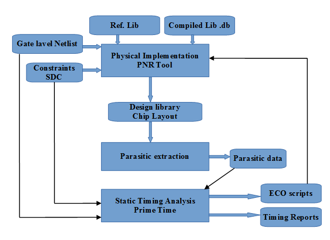
Static timing analysis is very important and faster way to analyze/verify all the timing paths at different stages of design. Other methods of timing analysis like simulation can verify that part of the design for which we provide stimulus. To verify all those timing paths with billions of gates is too slow and we are not able to verify timing completely. Figure 3. shows the basic STA flow with all required inputs as well as outputs which will be feed to PNR tool to solve Timing Violations and DRVs. STA tool like Prime Time by Synopsys needs Gate level netlist, SDC, SPEF, SDF, Library files as input. Output will be Timing reports and ECO tcl file, which is fed to PNR tool to implement in design with solved timing violations and DRVs.

ECO FLOW
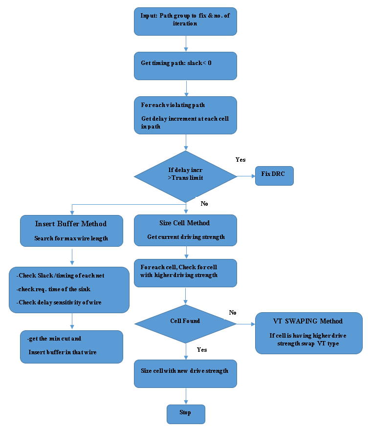
To meet the violation after implementing the design physically, the engineering change order is used. Eco flow is used to improve your Timing, DRVs, Power, Area and other constraints at any stage like post placement, post cts, post routing. There are two types of eco, all layer eco and freeze silicon eco. Mask generation is generally done after all layer ECO. In order to reduce significant cost after the tapeout phase the metal/base (silicon) eco is done in mask generation. The algorithm or techniques to solve the violation using ECO flow that we have used is shown in figure 4. As an input, we provide path groups to be fixed and the number of iterations. After analyzing the timing path, we will check for the slack <0. For each violating path, we have to check for the cell delay. In flow we stick to solve DRVs first and then timing.
There are basically four methods which can be used to solve timing like cell sizing, VT swapping, buffer insertion, and using Inverter buffer pair in clock network. In cell sizing method, we can derive the current driving strength of violating path cell and check for the availability of higher driving strength cell or alternate lib cell to replace the cell in order to improve timing. If there is no such alternative or higher drive strength cell available in library, we can go for second method that is VT swapping. In VT swapping we grep the combinational cells and swap their VT to ULVT, which also results into timing improvement. Third method is buffer insertion, to break the long net, which affects the capacitance of the net, and hence cell delay. After all eco fix has done, we can have the final eco data to run in PNR tool. The same ECO flow has been implemented in our design, the results and the effects are discussed in timing and pdv challenges section.

Other Challenges:
(A) Reduced Low Pin Count Testing
Due to shrinking in the size of chip to 28nm, 16nm, 7nm, and beyond, even the number of I/O pins on the processor increases where multiple types of test patterns (more logic gates to be tested) applied in multiple test cycles to achieve high test quality. To limit the use of number of pin-counts and reduction in the overall testing timing in a more efficient manner, DFT engineers are turning to new testability techniques to apply on a growing number of pin counts, and scan patterns in an efficient manner, such as reduced pin-count testing (RPCT) and also achieve maximum fault coverage.
Reduced low pin count testing is an effective solution that allows the application of at-speed test patterns using low-cost testers that are very pin-limited in order to achieve fault coverage and implementation testing time with minimal impact on design.
(B) Packaging Complexity
The original role of packaging was simply to protect the chips inside, but packaging is becoming every bit as complicated as developing a complex SoC(ASIC).
In the semiconductor manufacturing process, chip packaging is one of the most critical elements, which has flooded with innovation and complexity and particularly as the transistor size decreases. During packaging, lower technology nodes undergoes two condition: i) Leakage of sealed packaging. ii) Logical signals degrade when in contact. These nodes undergo critical packaging activities from start to finish which includes: wafer-level packaging (etching lithography and insulation), bumping, fan out, chip stacking, and other techniques that have contributed to the small-form-factor chips for high-speed functionality that client expected in mobile electronics and other technologies.
Conclusion
With time, in lower technology metal thickness, pitch, and cell height has scaled down, which has introduced new complexity in power planning. Also due to that it has introduced new IR/EM, timing, PDV, reduced low pin count testing and packaging complexity challenges. After going through these challenges PNR, timing flow, pin counts and packaging has been customized, which help us to mitigate the lower technology sign off challenges. So far we have discussed all the challenges and its solutions for the design closure to tapping it out on schedule, which is the key milestone to achieve for developing any ASIC. If you are looking for low power ASIC design assistance, we are here to help!


