Understanding PCIe 6.0
PCIe 6.0 supports a raw data rate of 64 GT/s (gigatransfers per second) and a maximum throughput of 256 GB/s for a x16 link, making it double the data rate compared to PCIe 5.0. While PCIe is used for internal data transfer with the processor through Direct Memory Access (DMA), it also allows communication between the processor and various peripheral devices connected to the PCIe slots on the motherboard.
While PCIe 6.0’s increased speed and throughput make it an ideal choice for connecting high-performance peripherals, ensuring the reliability of data transmission is crucial. So, Verifying the design becomes very crucial. With the help of the new PCIe 6.0’s Order Set (OS) error injection feature we can verify some of the corner cases of LTSSM (Link Training and Status State Machine).
What is PCIe 6.0 Order Set (OS) Error Injection?
Order Set (OS) error injection is a new feature introduced in PCIe 6.0 that allows for the intentional injection of errors into the transmitted/received OS. Before PCIe 6.0, error injection was not available inside the design, and engineers had to rely on external testbench components or third-party Verification IP (VIP) to inject errors.
With OS error injection, verification engineers have full control over the type, location, and frequency of errors injected into the transmission/reception. In a typical PCIe 6.0 setup, two devices are connected: a transmitter and a receiver. Before transmission, design can be configured on the type of error to inject, where to inject it, and whether the error should be repetitive. The designer can specify the lane, symbol, and byte location for error injection.
PCIe 6.0 technology uses a combination of a relatively lower First Bit Error Rate (FBER) of 10^-6 and a lightweight, low-latency Forward Error Correction (FEC) to achieve low-latency error correction. OS error injection helps create complex scenarios that might not occur in normal situations, allowing verification engineers to identify corner cases and verify the integrity of the design when faced with physical connection issues or repeated errors.
How OS Error Injection Works?
In PCIe 6.0, data is transmitted in chunks called order sets. There are seven main types of order sets: TS0, TS1, TS2, CONTROL_SKIP, EIEOS, EIOS, and SDS. Each order set consists of 16 symbols (except control skip which has 40 symbols), with each symbol comprising 8 bytes. The combination of different data within these symbols represents the order set.
To inject errors using OS error injection, verification engineers program control registers to define the target order set (e.g., TS1), the symbol within the order set (e.g., symbol 5), and the error pattern. The standard approach is to invert the existing value of the target symbol. Engineers can also define the frequency of error injection, such as injecting an error on the 1st order set and then again on the 9th order set and so on.
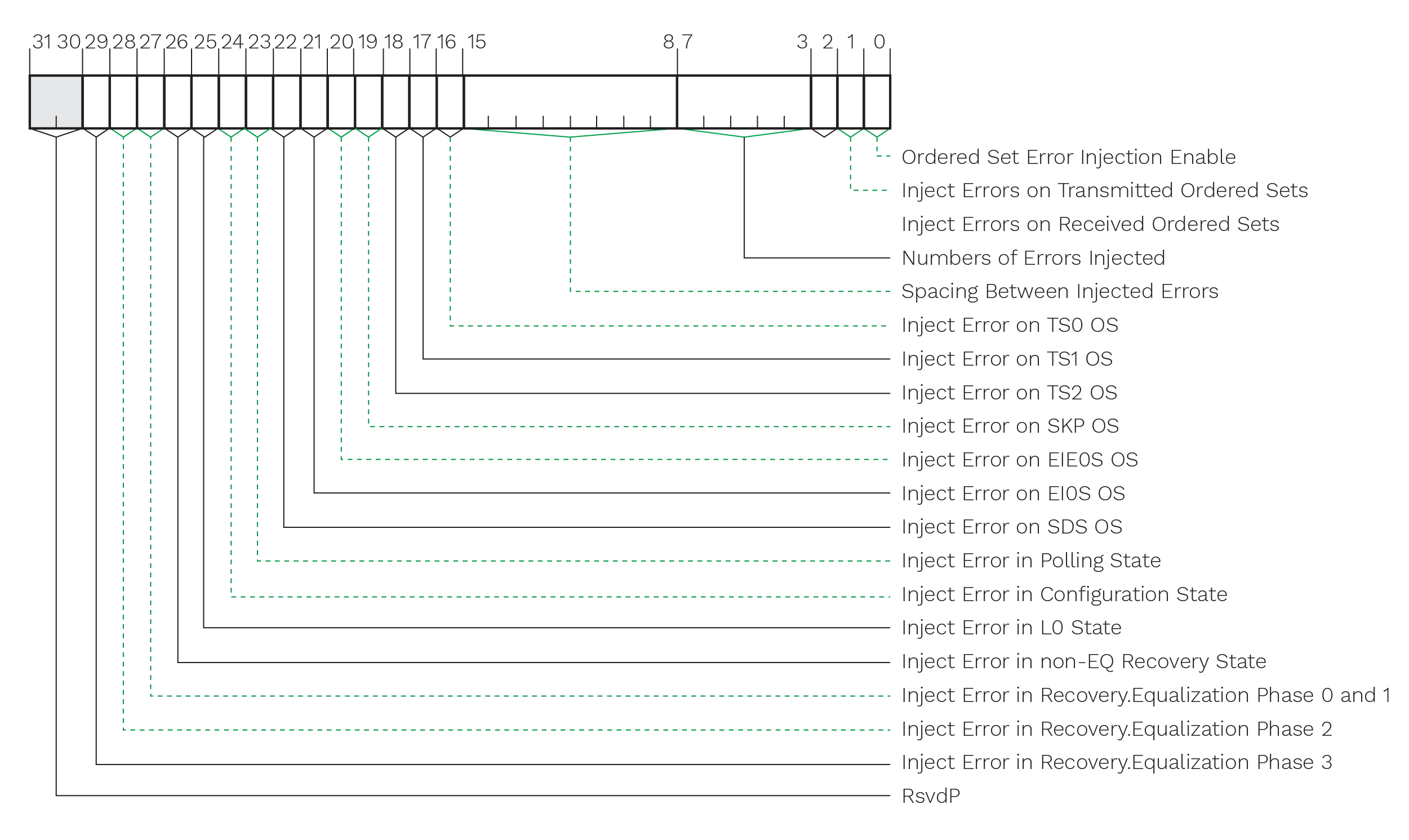
The 32-bit Control Register
At the heart of PCIe 6.0’s OS error injection lies the 32-bit control register.

As mentioned in the above section, this register allows verification engineers to configure various parameters to fine-tune the error injection process. Following are the control parameters:
- Error Injection: Enable/Disable
- Direction: Tx/Rx
- Data Rate: 2.5 GT/s to 64 GT/s
- No. of OS (Order Sets) to be injected with Error
- Spacing between two error injected OSs
- OS type
- LTSSM state
- Lane number
- Error Injection Byte
By adjusting these parameters, verification engineers can create highly specific error scenarios to thoroughly test their PCIe 6.0 designs.
Monitoring Error Injection with Status Registers
To keep track of the error injection process, PCIe 6.0 employs read-only status registers. There are two status registers – one for the transmission side and another for the receiver side.

These 32 bits read-only registers provide 2-bit output about the status of error injection for each order set. Let’s look at the possible status values:
| Status | Description |
| 00 | No error |
| 01 | Error Injection Started |
| 10 | Error Injection is Completed |
| 11 | Failure |
By monitoring the status registers, engineers can ensure that the error injection process is proceeding as intended and that their designs are responding appropriately to the injected errors.
Verification of OS Error Injection
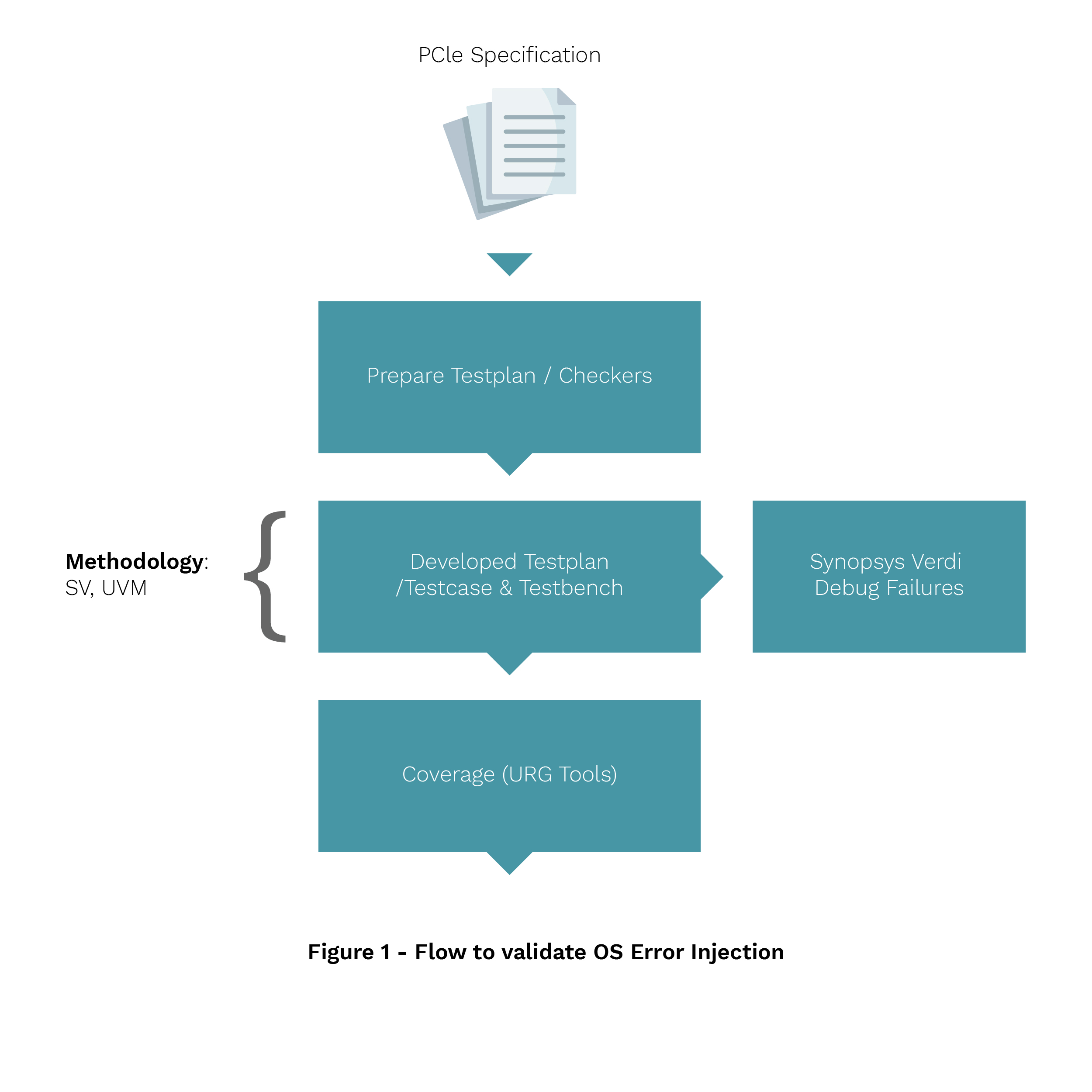
For verification of OS error injection, eInfochips follows the standard procedure to first read the specification and then based on specification; we plan the test plan for design verification. Based on this we plan the test cases and test bench. To effectively verify OS error injection in PCIe 6.0 designs, engineers often turn to the Universal Verification Methodology (UVM), a standard approach for ASIC verification.

A comprehensive verification environment for OS error injection should include the following components:
- OS Monitor
- OS Scoreboard
- OS error injection model
- Register model
By incorporating these components and planning test cases based on the PCIe 6.0 specification, engineers can thoroughly validate the error injection functionality and ensure the reliability of their high-performance PCIe 6.0 designs.
Conclusion
PCIe 6.0’s OS error injection capability is set to revolutionize design verification. By leveraging the 32-bit control register and monitoring the status registers, designers can create complex error scenarios to identify corner cases and ensure the robustness of their designs. As PCIe 6.0 gains traction in the AI world, mastering OS error injection will be key to developing reliable, high-performance solutions that can handle the demands of modern AI workloads. For more detailed insights, you can check out their approach to PCIe link training.


