This blog describes practical guidelines for High-Speed embedded hardware designers to enhance technical skills further on top of Engineer’s basics knowledge of Electronics, PCB design & manufacturing. It helps to answer several decisions making questions during the design phase regarding PCB material type, layout complexity & prediction of challenges, which can impact the product pricing and time-to-market of the product.
This blog is a perfect guideline for High-Speed embedded hardware designers to enhance their technical skills further in PCB design & manufacturing. It answers several decision-making questions during the design phase regarding PCB material type, layout complexity & prediction of challenges, which can impact the product pricing and time-to-market of the product
Explore the key questions addressed in this paper:
- Important terminologies for PCB material and how to select PCB Dielectric/core Material?
- How to select the Layer stack-up for high-speed interface applications?
- How vias are important (HDI/TH PCBs – Cost)?
1. Important terminologies for PCB material and how to select PCB Dielectric/core Material:
The below terminologies are used for high-speed PCB material selection:
a. Prepreg
Dielectric material (partially cured) is used to bond copper cores and copper foil in the layer stack-up.
Prepreg patterns (Woven Glass) [1]
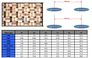
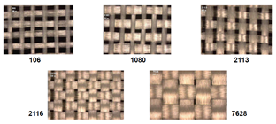
Fiber Weave Effects (affects timing parameter for High-Speed Signal) appear when PCB laminates with non-uniform properties. To mitigate Fiber Weave Effects, designers can use denser patterns i.e. 2116, 7628, 3113 etc.
The selected material shall have a higher resin factor, which indicates the closeness of resin and constant dielectric constant throughout the PCB. Variation in dielectric constant (lower Resin Factor) shall affect timing/propagation delay to high-speed or high-frequency signals.
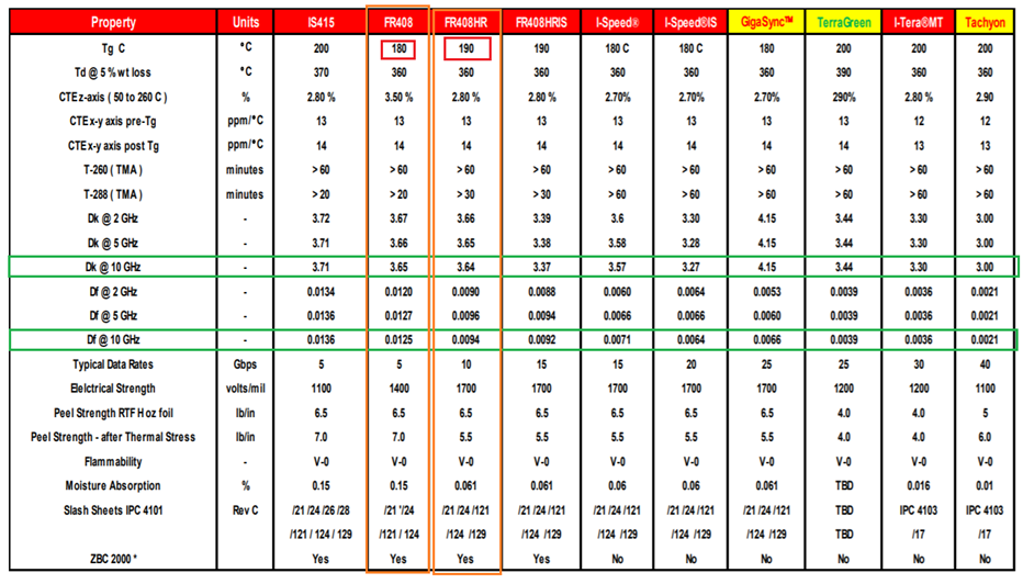
Df – Dissipation factor value has variations with resin content, type, signal frequency, and PCB trace testing methodology. The designer needs to verify the numbers thoroughly before finalization of a material. i.e.
The designer needs to check Df test measurement conditions and resin details from material supplier specifications to select material.
Df, Dk comparison for different materials is given in the next section.
b. Core
Core means a dielectric (with fully cured) between two copper foils.
Dk (Dielectric Constant) number for different Dielectric material can impact Impedance, Line widths, and losses significantly.
Dk, value is inversely proportional to propagation delay as per the below equation [2]

So, a Higher dielectric value will have a lower propagation delay which can support higher frequencies compared to a lower dielectric.
Refer to table [1] to understand how to verify Dk, Df values from the Datasheet of material and compare it between the two datasheets (follow the green, orange lines).
- Cost Factor w.r.t. material:
Below table describes how cost of PCB material changes as per Dielectric material.
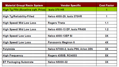
Note: Meet to the specification shall be on higher priority during material selection than the costing.
c. Copper foil and finish
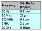
Cu foil is Cu used in the outer or inner surface layers of the PCB. The conductor does not have a perfectly smooth surface. The roughness/small tooth of foil increases bulk Cu resistance by 10% to 50% [1]. The electrical radiation increases when increasing the frequency or data-rate of interface used on board because skin depth decreased w.r.t. increasing frequency [1].
Type of Cu foils:
- DSTF – Drum side treated foil (tooth up to 10um)
- RTF – Reverse treated foil (tooth up to 10um)
- LP – low profile (tooth up to 9.9um)
- VLP – very low profile (tooth up to 5um)
LP/VLP Cu has lower roughness which can increase electrical performance compared to standard profile Cu. Loss characteristics improve with RTF/DSTF type of foils. For better impedance, VLP foils shall also be used.
Surface finish serves two purposes:
- Ensure solder-ability
- Protect copper against oxidation and corrosion
d. Construction
Construction indicates a PCB layer stack-up made from cores, a different type of material, prepreg (with a thickness of dielectric), Cu foil and finish.
2. How to select the Layer stack-up for high speed interface application?
Layer stack-up selection criteria:
a. Number of layers
Layer count can be added in even counts (2,4,6,8,12 etc.) only because copper layers can be added from both sides of PCB. It is to keep the overall layer stack-up symmetric.
The number of layers can be derived based on:
- silicon limitations e.i. ball grid array pitch
- silicon size and fanout complexity
- number of components on board
- overall complexity
- formfactor requirement
- layout guidelines
Note: The addition of every two copper cores to a PCB may add around ~25% to per board cost.
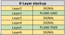
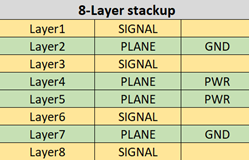
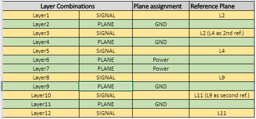
b. Layer Arrangements (signal and power layers)
It is important to meet electrical & mechanical performance for intended application.
Examples for 4-Layer, 6-Layer

8-Layer, 10-Layer stack-ups
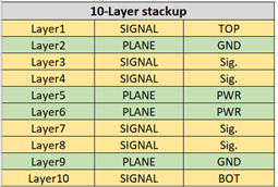
12-Layers
c. Manufacturability
The layout designer needs to follow each DRCs (Design Rules Checks) as per the manufacturer’s machine capability, which is very important during the Layout Design that drives PCB reliability and cost.
- Minimum copper trace width
- Copper to Copper minimum spacing
- Drill to Copper minimum Spacing
- Minimum Drill Diameter support
- Via to Via spacing
- Copper to PCB Edge spacing
- Type of Vias used
- Via on Pad
- Layer to Layer registration
Above all manufacturing capabilities drives the PCB manufacturing costs.
Note: As per current technology trends, in case of the requirements with less than 3Mil x 3Mil minimum copper to copper spacing, the designer needs to be relied on very few manufacturers around the industry. It can lead the product designer to increase the production cost due to strict requirement.
d. Thickness of copper layers & dielectric material
Material thickness can be measured in oZ/micro-meter/mil. The thickness of copper depends on the current rating & temperature rise requirement or temperature rating of the board. External copper layer thickness will include the plating thickness, which helps to have access current on top/bottom layers.
Online calculators are available to calculate the required Trace/plane width & copper thickness as per current.
Example: https://www.4pcb.com/trace-width-calculator.html
Note: Dielectric material thickness is subjective to trace impedances requirement. The fabricator can help designers to adjust the width of the dielectric based on requirement and DFM.
e. Trace impedance requirement
Trace impedance is completely subjective to silicon chipset manufacturer guidelines and impedance requirements for each trace/interface.
Traces on PCB derive calculated impedances (in manufacturer’s tools) based on trace width and spacing (between two traces for differential traces) to reference layers (strip-line and microstrip Traces).
Usually, below impedances across the industries are used:
- 42E (Single Ended): DDR/LPDDR
- 85E (Differential pairs): DDR/LPDDR (MIPI/UFS for Qualcomm)
- 90E (Differential pairs): USB, DDR
- 100E (Differential pairs): MIPI CSI, MIPI DSI, RJ45-LAN, HDMI
- 50E (Single Ended): eMMC, SDIO, SD card, RGMII, DMIC, RF(Wi-Fi-BT), NOR, all Low speed interfaces on board
- 120E (Differential pairs): CAN
Note: Actual impedance during manufacturing can vary by 5%/10% due to micro-level trace width changes (due to temperature variations) during the manufacturing process. PCB manufacturer generally verifies the impedances with impedance coupon (traces drown during design in a separate portion outside our required size of the board) during PCB manufacturing process.
The designer needs to confirm the RF Trace’s width/spacing to adjacent layer GND (as per 50E/chipset recommendation/ RF antenna recommended impedance) from the fabricator before proceeding for routing in the Layout. RF Trace’s width/spacing depends on the RF frequency running to the trace.
f. Board Thickness, Aspect Ratio:
- Any thickness up to 93 mils is considered standard (Thin Cores costs more) thickness. If the design has >250 Mil of thickness, then manufacturability needs to be reviewed again.
- Aspect ratio (PCB thickness/Minimum Drill size): Standard is 10:1.
Example 1: Through-hole board
PCB thickness = 63mil (1.6mm), Via Drill Size = 8 mil, then
Aspect ratio = 63/8 = 7.875 ; which is <10:1
Example 2: Blind via board
PCB thickness = 63mil (1.6mm);
Blind via Drill Size = 4 mil; Blind layers (i.e. L1 to L3 in 12 layers board) width = 20mil
Aspect ratio = 20/4 = 5; which is <10:1
Example 3: Board with a thickness of 200mil
PCB thickness = 200mil (5mm);
Via Drill Size = 8 mil;
Aspect ratio = 200/8 = 25; which is > 10:1; This case needs to be verified by Manufacturer.
Learning: In case of board width of 200mil, the Minimum Drill size shall be 20mil to maintain the Aspect ratio.
g. Via types
Refer to the following section.
3. How vias are important (HDI/TH PCBs – Cost)?
Vias are plated through-holes or plated laser drills that help to electrically connect traces from one layer to another layer on PCB.
The via types used on board can derive:
- Reliability of board
- Prototype costing
- Production cost
- Yield loss
- Time to market of the Product
The via types used on board can be selected based on Silicon chip/IC pad size, fan-out requirement, and electrical current requirement.
If fan-out can be done with through-hole (TH – 8C16 or 8C18) vias, then no need to use Laser (Blind/buried) vias.
Note: 8C16 means 8 mils of via drill size, 16 mils of via pad size (to meet manufacturer’s drilling capability)
Note: Check routing feasibility to confirm whether the board will be TH or BB Technology.
a. Current ratings for Vias
- Through Hole (8mil drill) = 1A / Via
- Blind Via (4mil drill) = 300mA / Via
- Blind Via with via Cu filling (4mil drill) = 950mA / Via
- Buried Via (8mil drill) = 1A / Via
Note: Above values are approximate at an ambient temperature of 55 deg. C and allowed temperature rise of 5 deg. C. Based on Copper plating thickness, the current rating may vary. Copper filling to vias is the best way to increase the current rating and reliability of the board.
There are tools available i.e., Saturn PCB Toolkit [4] to calculate different via’s current capacity based on the above parameters.
b. The designer can follow the below steps to analyze the via requirement for High-Speed Design
- In the case of BGA component on PCB, find a minimum pitch requirement for PCB out of all BGAs
- Check a via placement feasibility to check the signal fanout. Is it feasible to place 8C16 TH via considering a minimum copper to the copper requirement as per the fabricator?
- if yes, then the board can be fabricated with TH via only.
- If no, PCB needs a blind/buried vias.
See below image for Via placement in BGA for Fanout.

- If air gap between to pads of silicon is less than 9 Mil then it is mandatory to use Blind-Buried vias as per present PCB manufacturing trends/equipment technologies used with manufacturers.
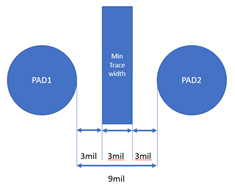
- The above drawing shows, the separation between two pads less than 9mils shall lead us to use blind buried technology on PCB.
- Layout board density and placement
Check the fanout feasibility after doing all placement on board. Make sure, no components placed below BGA fan-out section in TH via the type of boards. In case any requirement of placement complexity can lead the designer to move to Blind/buried via types on board.
c. Via type comparison w.r.t. reliability, cost, time to market
Below table shows the Comparison of Type of Vias with reliability, cost and time to market Ratings. This table may help the High-Speed Designer / Managers / Customers to decide the via structure or stack-up structure in the design

Note-1: Reliability rating is inversely proportional to the number of Process involved during Manufacturing Process.
Note-2: “Planarized” means, Layer to Layer Minimum allowable Resistance has to be set by manufacturer to stack Blind vias.
Note-3: “Any Via” Means Via can be put from any layer to any layer.
Note-4: Prototype cost compared as per past projects’ experience. It highly depends on the quantity of PCBs and vendor negotiation.
Note-5: “Number of Process involved” are derived based on Lamination cycles used as per PCB Manufacturing process.
Note-6: Manufacturing time is highly dependent on Number of Layers & complexity of board.
Summary
The PCB dielectric material shall be selected based on required reliability, maximum speed to be supported on board (with minimum loss), temperature profile, and assembly requirement. Actual selection can vary depending on the product’s requirement of temperature rating, reliability, application, compliance, and cost. Layer stack-up can be derived from the number of layers, the arrangement of layers, manufacturability, copper thickness, impedance requirement, Board thickness, and via types. Vias selection plays a very important role during stack-up selection because it can drive the reliability of the board, prototype costing, production cost, yield loss, and Time to market of the Product.
Designers can do feasibility analysis via selection through reviewing the silicon chip fanout from BGA, minimum pitch requirement, and layout density of the board. PCBs with only Through-hole vias can provide good reliability, lower manufacturing cost with an early time to market. PCBs with Any layer vias can provide the lowest reliability (higher yield loss), higher manufacturing cost with a late time to market (time taken due to manufacturing process complexity). PCBs with Blind (1-n-1 + TH vias can provide a medium level of reliability, medium costing with medium time to market (compared to the above two options).
Techniques described in this document can help the designers to improve the quality of the board and performance of interfaces for the product. eInfochips, an Arrow company, is a leading global provider of product engineering and semiconductor design services. For more information on PCB design solutions please connect us today.
Abbreviations
- BGA – Ball Grid Array
- CAN – Controller Area Network
- CSI – Camera Serial Interface
- DFM – Design for Manufacturability
- DSI – Display Serial Interface
- DSTF – Drum Side Treated Foil
- HDI – High Density index
- IOT – Internet of Things
- LPDDR – Low Power Double Data Rate (Type of SDRAM Memory)
- MIPI – Mobile Industry Processor Interface
- PCB – Printed Circuit Board
- RTF – Reverse Treated Foil
- TH – Through hole
- USB – Universal Serial Bus
- VLP – Very Low Profile
References:
https://www.microwavejournal.com/ext/resources/Webinars/2014/SLIDES_Isola_26feb14.pdf
https://blog.zuken.com/how-to-calculate-trace-length-from-time-delay-value-for-high-speed-signals/
https://www.4pcb.com/trace-width-calculator.htm

