Table of Contents

Q&A on ASIC-FPGA-SoC Design and Solutions

1. What is ASIC (Application Specific Integrated Circuit) Design in the Embedded world?

ASIC is a microchip, customized for a particular use or application. ASIC is classified into three types:

  1. Full custom ASICs
  2. Semi-custom ASICs
  3. Programmable ASICs

Reasons to use ASICs:

  1. Is small in size
  2. Provides IP protection
  3. Ensures low power consumption and efficient performance
  4. Decreases cost as chips size decrease
2. What is FPGA design?

FPGA stands for field-programmable gate array of programmable logic gates like AND or XOR and RAM blocks to implement digital computation in a best possible time interval. FPGA design is being used in various applications, including industries like Aerospace, Broadcast, Medical, Surveillance, Automotive etc.

3. What is FPGA prototyping?

FPGA prototyping referred to a hardware verification and quick software development. It is a technique which verifies functionality of ASICs and SoCs. It is widely used in handling the increased hardware complexity and software validation.

4. What are the reasons engineers prefer to choose ASIC over FPGA?
  1. One of the major problems that is faced with FPGA, compared to ASIC, is the high power consumption – which often becomes a limiting factor. Therefore, more effort is being spent to propose a design with low-power dissipation.
  2. Engineers prefer structured ASIC rather than spending time in optimizing the FPGA circuit layout into a single design mask for manufacturing. By having a fixed design like an ASIC, that is faster in deployment than an FPGA variable design deployment. It helps in saving time-to-market at the point of manufacturing and deploy the chip.
  3. Minimization of NRE (Non-Recurring Engineering) cost in ASIC design and fabrication is significantly lower than the FPGA. NRE includes cost of labor, tools, IPs, and masks in ASICs deployment.
  4. ASIC allows both analog signal and mixed signal design implementation. This is generally not possible in FPGA.
5. Why is FPGA prototyping required for emerging embedded technologies?

In advanced semiconductor design tools and methodology, an FPGA-based platform enables rapid creation of hardware-accelerated algorithms. FPGA-based prototyping has become an increasingly popular way of validating SoCs for many good reasons. To read more about why it is required, download the publication: FPGA Prototyping Trends and Challenges

6. What are FPGA slices?

FPGA slice is a collection of Configurable Logic blocks (CLB), of which FPGAs are made of. It consist of three components: Flip-flops, Look-up table (LUT) and Multiplexers. These components share connections within the SLICE.

7. What are the challenges in FPGA board design?
  • Not many designs fit in a single FPGA due to which design has to be partitioned across several devices. Initially, there were no tools for design partition, so this task becomes error-prone.
  • PCBs built to accommodate multiple FPGAs require numerous layers to verify connectivity for more than 10,000 signals and ping. This signal design mapping, will become error-prone and time-consuming. Without advanced methodologies and tools, bringing up an FPGA prototype will become longer.
  • After design partitioning and mapping, there are other issues that may arise in PCB physics like signal routing, capacitive loading, and impedance matching that will limit fast prototyping. Without good design techniques and reference designs, it is difficult to achieve efficient performance in one go.
  • Reusability is possible with FPGA boards, but difficult and time consuming to build for logical functions, due to which engineers typically do not get the advantage of quick development and reduced implementation risk for future projects.
8. What are the challenges faced in FPGA to ASIC conversion?
  • Design for testability in FPGA blocks are normally not an issue but critically important for ASICs blocks
  • Both FPGA and ASIC architectures handled with different clock distributions
  • Resets usage in control path and data path are often implied in FPGA, but not in ASICs
  • ASIC tool compatibility
  • Cost of changing a package from FPGA to ASIC is overpriced, if common packages chosen for both FPGA and ASIC then cost can be balanced

You may explore Resets in FPGA & ASIC control and data paths, which are normally followed by design engineers to choose the appropriate reset type and usage in their designs.

9. What is the need for spice simulation in mixed-signal SoC design?

The semiconductor industry is looking for high capacity and high-performance circuit simulation to support memory applications, and lower technology node design in analog and mixed-signal devices

Analog /Mixed-signal design applications are the fastest growing segment in the semiconductor industry. Engineers face challenges when it comes to interaction between analog and mixed-signals. During the interaction, engineers are often faced with the problem of memory design implementation, which requires SPICE (Simulation Program with Integrated Circuit Emphasis ) SIMULATION to support in validating circuit memory design. It is open-source analog electronic circuit simulator used to check the integrity of circuit designs and to predict circuit behavior and functionality.

Spice simulation is one of the efficient approach which is required in debugging mixed-signal SoC (ASIC) design with Verilog-A/MS modeling . With the right approach, it also helps in simulation time, speed and accuracy option in SoC verification. For right spice simulation, certain rules are being followed by engineers to avoid budget losses in mixed-signal SoC design.

10. What are the quick ways to overcome FPGA to ASIC conversion challenges?
  • Best to use IP that can be synthesized on FPGA prototyping.
  • Due to asynchronous RAM access and asymmetric I/O ports with different word widths FPGA I/O ports and RAM cannot be replicated into ASIC. In that case, extra wrappers and logic need to be added to make an equivalent cell on ASIC.
  • There are many front end tools (Code checker and least-common-denominator coding style) to be used by engineers for ASIC synthesis and FPGA synthesis which helps in avoiding software (Code analysis) mismatches in results.
  • Verify test benches extensively in logic gates connectivity, clock frequencies, and timing differences while converting from FPGA to ASIC.
11. What are open-source tools being often used in ASIC design?
  1. For Simulations- Xilinx Vivado, Mentor`s ModelSim.
  2. For Logic Synthesis- Yosys
  3. For Floor Planning, Placement, and CTS- Graywolf
  4. For Routing- Qrouter
  5. For STA- Open Timer
12. How does FPGA synthesis works?

FPGA synthesis can be done with a set of tools such as Xilinx Vivado, Altera Quartus, Synopsys FPGA Compiler etc. It follows three basic steps:

  1. Compiles and creates a design of the hardware representation of the logic and registers.
  2. Converts the representation of a design to the target hardware without worrying about time because at the same time synthesis
    tool will try to make the smallest design with best possibilities.
  3. Compares the logic paths in the design with timing optimization.
13. What is a logic cell in Xilinx FPGA?

LUT – Look up table is a logic cell in Xilinx FPGA. It is a small memory which is having same functionality just as ROM that can generate 4-input Boolean functions (AND / OR / XOR / NOT / and its combinations)

14. What is Mixed-signal ASIC design?

Mixed-signal ASIC design is an implementation of analog and digital circuit on a single semiconductor integrated circuit, which shares a common power supply. This integrated circuit is considered as a cost-effective platform for building smart electronic applications.

Know more about various aspects of Mixed Signal design debugging steps and methodology.

15. What are the challenges faced by Digital ASIC Design engineers in Mixed-signal Integrated Circuit design?
  • Run simulation over hundreds of clocks in order to set-up mixed-signal design (PLL setup, real-time configuration, calibration)
  • Check the functionality of SoC and non-ideal behavior of A/RF sub-systems
  • Analyze high ratio of carrier to the modulation frequency
  • Debugging process from A/RF system specification through to silicon testing
Looking for an able partner to tackle your ASIC design & FPGA-SoC Development challenges?
Let’s Connect
16. What are the benefits of mixed signal asic design?

Top 5 benefits of Analog and Mixed Signal ASIC design are:

  1. Low cost
  2. Lower geometry design
  3. Increase in performance
  4. Low Power
  5. Reliability improvement and maintenance
17. What makes verification in SoC level so difficult?

The key challenges of SoC verification are:

  1. Ever increasing functionality and complexity of the SoC and shrinking time to market
  2. Increased simulation cycles
  3. Most of the designs today include various sensors and actuators along with the digital design; therefore, it is imperative to do Analog Mix signal simulations
18. How to verify a complex clock system in SoC verification?

As the technology is getting advanced, the complexity of SoC is also increasing. It consists of multiple wireless modules with various interfaces like I2C, PCM, I2S, AHB. All these modules, which support a range of clock frequencies, which must be checked to ensure that they operate without a glitch. A clock monitor can be used to verify the complex clock systems.

A clock monitor is an SV/UVM based component to monitor the clock under test. As the functionality of the clock monitor is unique and flexible, we can reuse it on different types of SoCs.

Know more about the functions and advantages of a clock monitor.

19. What is a good Analog / Mixed-Signal Verification Methodology?

With the complexities in digital designs / SoCs, it is required to automate methodology to face challenges in mixed-signal verification and debugging in AMS verification cycles. Some methodologies being used to verify Analog / Mixed Signal Designs are:

Method 1: Using low level nonfunctional behavioral model.

Method 2: Using an analog functional behavioral model developed in VHDL or Verilog AMS language.

The proposed methodology provides complete functional verification for Analog / Mixed Signal Design. To know in detail, click here.

20. What are the common issues faced by engineers in an ASIC verification environment?

Some of the common challenges faced by ASIC verification engineers in the semiconductor industry are:

  1. Aggressive verification schedule, with ever-increasing design complexity and shrinking time to market.
  2. Staying up-to-date with knowledge of different methodologies and technologies involved in verification, including UVM, hardware protocols, architecture, UPF, AMS, CDC, CRV and CDV.
  3. Testbench architecture development to effectively reuse and enhance the testbench for future use.
  4. Automation of regression flow and error reporting.
  5. Finding ways to reduce long simulation time for real use cases.
21. What is post-silicon validation?

Post-silicon validation is a vital verification phase. It makes use of a fabricated, preproduction silicon implementation of the target SoC design on which variety of tests and software are run.

22. What are the types of post-silicon validation testing?

Post-silicon validation is used to detect and fix bugs in integrated circuits and systems after manufacturing testing. In order to detect bugs, the below functional tests are performed:

  1. Per Pin Testing
  2. Parametric Testing
  3. Functional Testing

Know more about these approaches for the test scenarios.

23. Why adopt Model-based Design?

In order to improve product quality and decrease time to market, it is recommended to adopt Model-based design (MBD), which performs verification and validation (V&V) through testing in the simulation environment.

24. What is the use of multibit flop and what challenges does its usage bring in ASIC Physical design?

In the VLSI industry, the continuous need of lower technology node presents all the ASIC layout engineers a challenge to design integrated circuits with better quality performance, lower power consumption and lesser cost.

In order to reduce the power in ASIC without affecting the performance of the integrated circuit design, Multibit flops are recommended.

There are many other advantages while using multibit flip-flops like:

  1. Reduction of clock power
  2. Better clock tree from the same clock gating cell
  3. Less buffer, which improves routability.

Know more about the challenges and solutions of Usage of multibit flops.

25. How are mixed signal assertions different from digital assertions?

For Digital verification, standard assertion languages like PSL and SVA are used in discrete domain. However, mixed signal verification system will need to extend the principles of ABV and add some control for a continuous domain. For verifying analog quantity like voltage, current, etc., we should use the Verilog-AMS or Spectre/SPICE languages.

There are three types of assertion techniques in mixed-signal verification:

  1. Verilog-AMS based Assertions
  2. Specter simulator based Assertions
  3. Using Property Specific Language (PSL) with Verilog-AMS

Read more about the above-mentioned assertion techniques in detail.

26. How to overcome difficulties and speed-up the SoC design verification?

SoC (System on Chip) level functional verification flow is a process, which describes efficient ways to speed up the system-on-chip (SoC) design process. To ensure successful tape-out of SoCs, here are the steps of a standard SoC-level Functional Verification flow: click here.

27. How to overcome difficulties in verifying clocks in complex system-on-chip (SoC) or IPs?

In SoCs, the clock control unit is critical and their components share a single clock unit, which generates various clock inputs for IPs and protocols, enabling them to function seamlessly. In order to understand the functionality of a clock monitor that can verify complex clock systems read about the concept of clock monitors in SoC verification.

28. What are the various types of power dissipation techniques in lower geometry design?

In VLSI technology, the shrinking of the devices, power dissipation has emerged as an important factor while considering efficient performance and area lower geometry chip design. In this day and age, everybody needs a sleeker device with more capabilities and longer battery life. Learn about the types of power dissipation and techniques to prevent the voltage on lower geometry design. Know more.

29. What is CMOS output?

What is CMOS output? CMOS output consists of two signal specifications i.e. High output stage and low output stage where the CMOS gate is operating at a power supply voltage of 5 volts. Due to the addition of CMOS output, the need of additional step-up circuits and external capacitors is not required.

30. What is programmable logic controller (PLCs)?

The Programmable logic controller is a control system for industrial automation of electro-mechanical process. These controllers perform multiple functions like: analog and digital input and output interfaces; signal processing; data conversion; and various communication protocols. For more details, read semiconductor technical documents.

31. What are SoC design challenges?

System-on-a-chip consist of both controllers for microprocessor and microcontrollers. The major challenges of soc design are:

  1. Architecture Strategy
  2. Design testing Strategy
  3. Validation Strategy
  4. Synthesis Backend Strategy
  5. Integration Strategy
  6. On chip Isolation


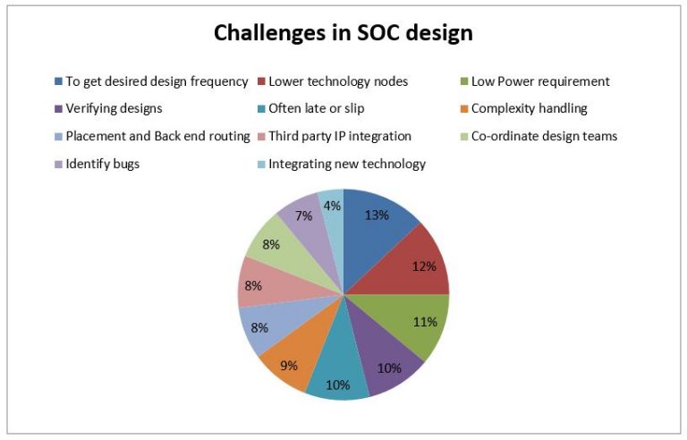
To overcome the above-mentioned challenges (Image 1), ARM has designed a program called ARM Approved Design Partner, which enables ecosystem partners in specific technologies and activities to support their customers better.

Also, eInfochips has developed stringent processes and infrastructure to handle complex turnkey ownership. Know more about the ability of the SoC device to perform at low power.

32. How to improve the design verification of complex System-on-Chip (SoC) design?

To speed up the SoC verification process with a successful tape out, engineers need to follow the SoC design and verification flow given below which defines the five essential steps:

  • SoC Level/Top Level view (Feature Extractions)
  • SoC Level Verification Plan
  • SoC Level Verification Environment and SoC Verification
  • Functional and Code Coverage Closure
  • Final Functional Verification Closure (Verification Sign-off)

In order to provide noteworthy benefits to enterprises, read the above-mentioned steps in detail here: What is SoC Design Verification Flow?

33. How does FPGA provide noteworthy benefits to enterprises?

As customer demand keeps on changing, manufacturers need to change or upgrade their products to stay relevant. FPGAs are designed to provide the required flexibility and make changes to the product functionalities at any point even after deployment at the customers’ end.

Adoption of FPGAs has been driven by the concept of combining the best features of ASICs and processor-based systems. FPGAs can be leveraged across various industries to provide multiple benefits, like parallel processing, reduction in total cost of ownership, simple design cycle, flexibility, reusability, and faster time-to-market. To help businesses leverage FPGAs to its fullest potential, eInfochips has partnered with companies like Intel, Microsemi, and Xilinx. Here’s the blog, which summarizes the main benefits of FPGA to enterprises.

34. What is Synopsys’ Hierarchical Verification Plan (HVP)?

Hierarchical Verification Plan (HVP) using the Synopsys’ Unified Report Generator (URG) facilitates an easier and more efficient way to track the verification progress. Hierarchical Verification Plan (HVP) provides a deeper visibility into the regression process and coverage analysis.

Know more about the flow of the Hierarchical Verification Plan creation in excel format, along with the detailed steps for integration of the same in the verification environment with suitable example.

35. What is RTL verification?

RTL stands for register transfer level. This functional verification helps to reduce syntax errors from VHDL code and ensure that the code is logically correct.

click here to know about how to manage RTL to GDSII implementation projects involving advanced process technology nodes and low power design techniques.

36. What are the challenges faced by designers who need to prototype SoCs?

Design challenges faced by engineers while prototyping SoCs are as follows:

  1. Design partitioning.
  2. Bringing techniques and tools in order to overcome physical problems, design errors, or mapping issues.
  3. Difficulties in debugging.
  4. FPGA-SoC prototype board design performance consideration and its impact.
37. What are the advantages of FPGA prototyping?

The major advantages of FPGA prototyping are:

  1. VHDL is tested with real clock speed, in real environment
  2. Prototyping environment offers “early ASIC” for other projects
  3. More secure to sign off
38. How to avoid routing congestion in FPGA product design?

In FPGA product design, congestion needs to be analyzed. The results of routing largely depend on how congested your product design. Following are the few techniques with which design engineers can control the routing congestion in FPGA product design

  • Placement blockages
  • Cell padding
  • Macro padding
  • Maximum Utilization constraints

Read more about these techniques in detail, here.

39. What is the difference between global and detailed routing?

The routing problem in the design of integrated circuits is resolved by a two-stage approach of global routing followed by detailed routing. Global routing divides the routing region into tiles for all the nets, then generates a tile-to-tile path to connect the pins. As per the paths obtained in global routing, detailed routing assigns actual tracks and vias for nets. Read more.

40. What is ASIC design flow?

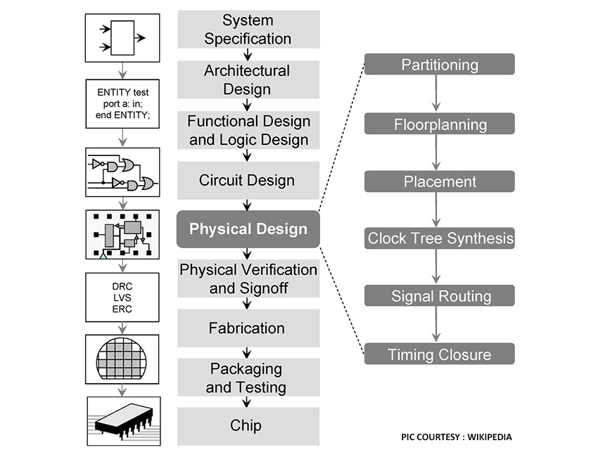
ASIC design is based on the flow that uses HDL for designing and applied to Verilog and VHDL.  It includes the following steps of the flow:

  1. Size, Power Consumption and Performance Specification
  2. RTL Coding
  3. Simulation
  4. Synthesis
  5. Pre-layout / Post-layout Timing Analysis
  6. Automatic Place and Route Process (APR)
  7. Back Annotation
  8. Logic Verification
  9. Tape-out


41. What are the tools used by engineers in ASIC design flow?

Some of the tools or software used by ASIC design engineers in the back-end of ASIC design flow are listed below:

  • Cadence (SOC Encounter, Innovus , Voltus,)
  • Synopsys (Design Compiler, ICC/ICC2)
  • Mentor Graphics (Olympus SoC, IC-Station, Calibre , Talus)
  • Redhawk Apache
  • Conformal LEC
  • Synopsys Primetime
42. What is STA in ASIC design flow?

STA (Static Timing Analyzer) in ASIC design flow is a simulation process of computing the unexpected maximum and minimum timing delays in your design. The timing analysis checks are done by using timing analysis tools (Synopsys Primetime, tempus) in the integrated circuits.


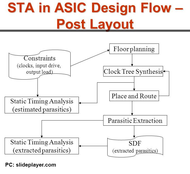
  • Performing STA at two stage
  • Pre layout STA
  • Post layout STA
  • Pre layout STA after synthesis
  • Post layout STA after routing and in sign–off
43. What are the benefits of using SoC?
  1. Lower geometry designs
  2. Reduced system costs
  3. Lower power consumption
  4. High impactful performance with minimal risks
Empower your Products with eInfochips-Intel FPGAS and SOCS?
Let’s Connect
44. Which are the best DFT techniques?
45. What are the Challenges in Low power Verification?

Low Power Verification challenges include following:

  1. Power controlling and monitoring
  2. Power gating and power-up operation in each block
  3. Power gating and power retention in memories
  4. Multiple low power modes and mode transition
  5. Low power integration of Hard macros and analog IPs
  6. Impact of clock frequency switching
  7. Test mode checks for design and analog IPs

To overcome these challenges, here are some approaches related to front-end HDL based design styles, which can reduce power verification, mostly unravel techniques that are considered quite trivial, yet have a significant impact on the overall power consumption.

46. What is UVM Verification Methodology?

UVM stands for the “Universal Verification Methodology”. It is a standard verification methodology from the Accellera Systems Initiative that was developed by the verification community for the verification community.

UVM represents the latest advancements in verification technology and is designed to enable the creation of robust, reusable, interoperable verification IP and testbench components.

You can also refer the following link for the same/more detail.


47. Why is DFT Required in VLSI Industry?

DFT (Design for Testability) is required for post-production testing of the chip design process to make the production 100% error-free.

As the semiconductor industry is progressing towards lower geometry design, reduction in voltages, complex macrocells, and reuse of existing one, these changes require reliability and quality, which is why DFT is required in VLSI (Very-large-scale integration) industry.

48. Why is FPGA Prototyping Required?

SoCs incorporate increasingly complex hardware features with more software application, which makes the process of validating SoC challenging. FPGA prototyping helps in validating complex SoC. It is a well-established, reliable technique for verifying the functionality and performances of ASIC/SoC and early software development, which is the reason why FPGA Prototyping is required.

49. What are the Cadence tools used in ASIC design flow from RTL to GDSII Services?

Following are the Cadence tools used in ASIC Design flow:

  • Synthesis: Genus
  • Place & Route Implementation: Innovus
  • Timing Sign-Off: Tempus
  • RC Extraction: Quantus QRC
  • IR Drop analysis: Voltus
  • Logical Equivalence / Low Power checks: Conformal
50. What are the best low-power implementation techniques in ASIC design?

The best 5 low power techniques in ASIC design are:

  • Clock gating
  • Power gating
  • Power-aware memories
  • Multi-threshold design
  • Multi-voltage design
51. What are the SoC Design Level Challenges in IoT applications?

The soc design level challenges in IoT applications are:

  • Power management
  • Use of Adaptive Voltage Scaling and its management
  • Speeding through Wireless standards certification
  • Different connectivity of protocols per chip like sensor interface due to diversity in devices.
  • Increase in complexity of design and standards verification
52. How to achieve faster time-to-market in ASIC Design Services?

For a continuous performance of ASIC design, hardware designers need to reduce time-consuming manufacturing cycle, to reduce the overall product development costs. Here’s the infographic that showcases how to achieve faster TTM in ASIC design.

53. How does eInfochips help in the ASIC design environment?

eInfochips has introduced OptiX, an ASIC design environment tool for a full-chip design environment that includes:

  1. Configuration of ASIC flow from RTL to GDSII
  2. Reducing risk and accelerating productivity
  3. Configuration of library and foundry files with the support third party tools

To know more about how OptiX can help, download this case study – OptiX – ASIC Design Environment Tool.

54. How does eInfochips help in mixed signal board designs of IoT applications?

The mixed-signal design for the IoT includes the ARM IoT Subsystem of Cortex-M processor families, along with Cadence’s interface IP and unified mixed-signal implementation technology, optimized for Cortex-M cores. ARM has released an Approved Design Partner program, endorsing eInfochips for designing embedded or connected IoT products.

55. How eInfochips helps in ASIC/FPGA design and development services?

eInfochips offers custom ASIC design, FPGA development, design V&V and physical design with DFT architecture to help clients meet low volume and faster TTM requirements.

eInfochips’ team of engineers has helped in 180+ successful silicon tape-outs. In an era of miniaturization, eInfochips has enabled multiple tape-outs from 180nm to 16nm, currently working on 7nm with 99% of coverage.

Get a quick prototyping service for multi-million ASIC into multiple FPGAs to turn around a proof-of-concept for showcasing to your end customers. To know more, visit the page.

To know more about the approach and trends that influence the use of FPGA prototyping,  check out this publication on FPGA Trends & Challenges.

Explore More

Talk to an Expert

Subscribe
to our Newsletter
Stay in the loop! Sign up for our newsletter & stay updated with the latest trends in technology and innovation.

Our Work

Innovate

Transform.

Scale

Partnerships

Device Partnerships
Digital Partnerships
Quality Partnerships
Silicon Partnerships

Company

Products & IPs

Services