In VLSI, physical design (is also known as integrated circuit layout) is a process in which the front end design transfer the structural netlist to the back end design team to convert into a physical layout database which consists of geometrical design information for all the physical layers which is used for interconnections.
The physical design process encompasses several pivotal steps:
Floor planning: This initial step involves determining the overall structure and dimensions of the chip. It includes allocating space for different functional blocks and deciding on the optimal placement of these blocks to meet performance and power objectives.
Placement: Following floor planning, individual components such as transistors, gates, and flip-flops are placed within the designated regions. The objective is to minimize physical distances between components to optimize performance while considering factors like power consumption and heat dissipation.
Routing: Once placement is finalized, the next step is routing, where interconnections (metal wires or traces) are established between the placed components to facilitate the flow of signals. This step involves solving complex optimization problems to minimize signal delays, power consumption, and other performance metrics.
Clock Tree Synthesis: Ensuring a reliable and efficient distribution of the clock signal throughout the chip is crucial for synchronous circuits. Clock tree synthesis involves creating a hierarchical structure of clock distribution networks to minimize clock skew and optimize performance.
Power Planning and Analysis: Given the significance of power consumption in modern IC design, this step involves techniques such as power gating, voltage scaling, and optimizing power distribution networks to minimize overall power consumption.
Physical Verification: Once the physical design is complete, the layout undergoes various verification steps to ensure adherence to design rules, compliance with manufacturing constraints, and absence of potential issues such as shorts, opens, and timing violations.
Physical design is a pivotal stage in the overall IC design process, playing a significant role in determining the final performance, power efficiency, and manufacturability of the semiconductor device. Semiconductor designers employ specialized tools and methodologies to efficiently carry out the tasks involved in physical design.
DRC is a process where the entire physical design database is checked against design rules. The design layout must adhere to the standards defined by the foundry for manufacturability. DRC was introduced as the lower geometry design technology has evolved vigorously. Understand how design rule checks are applied for 28nm node technology: https://goo.gl/afrNKd
This question is often asked in context to explain how design rule checks can be applied in lower technology nodes on the block and full-chip level.
Design rule checks are nothing but physical checks of metal width, pitch, and spacing requirement for the different layers which depend on different technology nodes. DRC helps in fixing up chip design by checking logical connections of all IC components with design rules and reports, and if they fail, the chip won’t be able to perform specific tasks.
There are some techniques that need to be followed to fix-up DRCs for lower technology nodes. Following are:
- Short violation
- Spacing violation
- Same layer spacing with net and cell geometry blockage
- Minimum chip area requirement
- Misalignment of VIA
Understand how the above-mentioned design rule checks in detail for lower technology nodes: http://bit.ly/2YK8OjR
IR drop is a voltage drop, which affects technology node performance. The power supply in the chip is applied uniformly through metal layers. When voltage is applied to these metal wires, power starts flowing through these metal layers. At that moment, some voltage may get dropped due to the resistance of metal wires and power supply. This drop is called IR drop.
IR drop determines the level of voltage drop in the wires that reaches the pins of standard cells. Value of acceptable IR drop will be decided at the starting of the project and it is one of the factors which determines the performance and reliability of digital IP blocks in lower geometry designs.
If the value of IR drop is more than the acceptable value, it will cause failure of electronic boards due to overheating.
Learn more about IR drop issues and techniques to prevent such issues in the electronic devices.
- The high impact of manufacturing cost and the need to get the design right in the first run
- Managing double patterning (DP) is difficult i.e., Restrictions and alignment issues on the circuit design layout.
- Design rules check are highly complex for engineers to memorize, when there are more than 5000 rules, and several checks for the lower geometry design and verification.
- Drain Induced Barrier Lowering (DIBL) is another challenge faced by physical design engineers in lower geometry design. It is a short-channel effect in MOSFETs, referring to a reduction of the threshold voltage of the transistor as the drain voltage goes high.
- IR drop and Electromigration issues are becoming common now in small chip design while moving towards 16nm, 7nm, and beyond whose effect can damage the electronic device and shorts due to high current density supply in circuit.
- Optimized costs in Lower geometry chip design by using suitable DFT techniques, double patterning, mask making, use of 3D ICs, etc.
- Applying big data analytics in chip manufacturing to improve quality and performance of each component of electronic circuit.
- Following efficient integration and faster decision making in end-to-end supply chain management and faster time-to-market.
- Minimize custom flows and shift towards P&R flows for better physical data-path capabilities.
- Focus on reducing the risk of functional failures of the design to prevent business stoppers.
- Adopt better methodology (OVM, UVM, AVM, etc…), and advanced tools (Innovus, Synopsys ICC2).
With the increasing demand of lower technology and low power consumption, eInfochips provides physical design service (RTL-to-GDSII-to-DFT) capabilities.
eInfochips offers DAeRT tool in DFT services for ASIC designs. DAeRT (DFT Automated execution and Reporting Tool) is a framework that gives a platform to create DFT (Design for Testability) flow. It helps to achieve ~100% testability for the ASIC designs.
“DAeRT” supports various DFT methodologies starting with IJTAG/JTAG, MBIST, Scan, ATPG, Pattern Validation, Test Timing Analysis, and Post-Si validation. Know more about the tool in detail:http://bit.ly/2GM32UD
Design classification based on system/package type:
- System on package (SOP)
- Package on package (POP)
- Wirebond package
- Flip-chip package
For more information on physical design and tape out requirements, go to: https://goo.gl/xf20xc
![5 Proven Tips for Right Time-to-Market at 16nm Lower Technology Node [Infographic]](https://www.einfochips.com/wp-content/uploads/2017/06/5-proven-tips-for-right-time-to-market-at-16nm-lower-technology-node.jpg)
To know more about the impact of 16nm in the IoT era, visit the blog: 5 Proven Tips for Right Time-to-Market at 16nm Lower Technology Node [Infographic]
Power requirements are very critical in modern networking ASICs. In VLSI, advanced techniques like MBIT flops and MIMCAPs can help improve the power and area numbers in 16nm design.
By replacing and merging single bit flops with multi-bit flip-flops using different algorithms, it significantly reduces the area and power numbers for ASIC designs. On-chip MIMCAP (Metal Insulator Metal capacitor) reduces the voltage fluctuation and noise on the power supply, which may have affected signal integrity, reliability, and speed of design. To know more about these advanced technologies, click here.
Physical design implementation challenges include:
- Floor planning
- Power planning
- Placement
- Clock tree
- Routing
- Physical Verification
- Timing closure
- Sign-off
To read more about above-mentioned points in implementing a flat design, click here
FinFET has higher drive current in comparison to SOI. Moreover, the strain technology in FinFET can be used to increase carrier mobility. Below are the strengths and weakness of SOI and FinFET in micro-electronics industry:
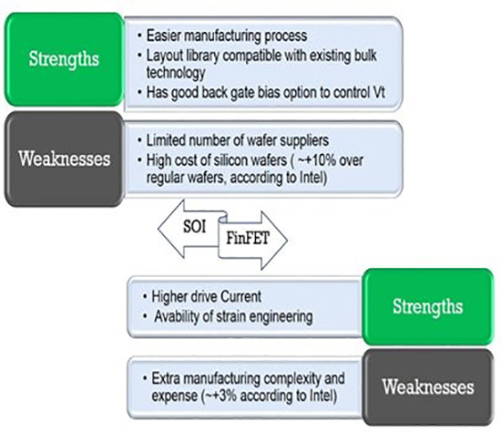
Read more about the importance of CMOS, SOI and FinFET Technology in the micro-electronics industry.
It is a process of arranging a PCB layout to mitigate difficulties that can come up during PCB fabrication, test, procurement, and assembly functions, which are part of the manufacturing process of an electronic system.
- Reduce the number of parts
- Development of modular design
- Use of standard components
- Design for ease of fabrication
- Minimize assembly directions
- Minimize compliance
- Lower production cost
- Higher quality
- Quicker time to market
- Lower capital equipment cost
- Greater automation potential
By doing DFM analysis in the PCB layout process, the PCB design cycle time is directly controlled by the designer as a part of the design process. This improves the cycle time, which is needed to iterate through the process of resolving manufacturing violations.

Read more about DFM analysis and its integration into the design system
The top 10 contributing factors to DFM are as follows:
- Product complexity
- Product variants
- Components availability and price
- Reusability of design
- Failure analysis techniques
- Managing design cost
- Incorporating last stage design changes
- Production of friendly design
- Product quality and regularity requirements
- Quality standard framework
Read about DFM contributing factors in detail.
Semiconductor industry introduced different tools and techniques to control and monitor product quality and performance. Wafer-Level Reliability test is considered as one of those techniques which can be used to provide fast feedback information regarding the reliability of the product in a semiconductor process. This feedback includes process control monitoring (PCM), process qualification, reliability control monitor (RCM), and quarterly monitoring (or re-qualification).
In ASIC design flow, we are performing different stages such as floor planning, power planning, placement, clock tree synthesis, routing and final signoff. Among them, one of the most important stages is building the clock structure for a flip-flop. It is a process of providing the clock connection to the clock pin of a sequential element.
- Clock tree synthesis (commands for building clock definition)
- create_clock -name clk -period 100 -waveform{0 50} [get_pins{xtal_inst/OUT}]
- create_clock -name clk -period 100 -waveform{0 50} [get_ports{clk}]

Get silicon tape-out solutions across lower technology nodes Click Here
Clock gating is a technique that reduces the switching power dissipation of the clock signals. By inserting a clock gate circuitry, unnecessary clock switching of adders can be avoided during the clock cycles and the stored data remain unchanged. The condition under which a clock signal passes through the clock gate is known as Enable Function, which is the input of the EN port of clock gate circuitry
It is the most popular method for power reduction of clock signals and functional units. A significant fraction of the dynamic power in a chip is in the distribution network of the clock.
Know more about power reduction methodologies in this Low Power Design for Testability
Watch the below 6-minutes video to know how eInfochips helps in m2m IoT application development with low power clock tree synthesis (CTS) optimization in ASIC back-end solution platform.
Electromigration is the gradual displacement of metal atoms in a semiconductor. It occurs when the current density is high enough to cause the drift of metal ions in the direction of the electron flow, and is characterized by the ion flux density. In small die size chip, there is a requirement of high density, which creates a momentum that transfer from moving electrons to the metal ions. These ions will drift in the direction of electrons and result in the displacement of metal atoms, which causes open and short circuits.
Electro-migration is a movement of ions in semiconductor material on chips that engineers need to optimize, especially in lower geometry designs. Integrated circuits need to be reliable and that is why engineers need to understand why they fail. Many issues faced by engineers due to Electromigration include:
- Timing violation (setup/Hold)
- Low current density
- Current flow via arrangements (Wire shapes, corner bends)
- Current distribution within device pins
- Temperature of the chip
Know more about electromigration in physical design.
Important manual fixes that engineers need to understand in ASIC physical design to overcome the risk of electromigration are:
- Driver Downsizing, which will reduce the current density in the interconnects
- Non-Default Rule (NDR) on the victim nets, which will increase the width of metal and will also increase the current carrying capability
- Routing of higher layers due to high current capabilities
- Multi-cut Via or Non-Default Rule (NDR) in order to increase wire reliability
Physical synthesis begins with a mapped netlist generated by logic synthesis.The netlist describes the logical connections among the physical components (logic gates, macro/IP blocks, I/O pins, etc.). Physical synthesis generates a new optimized netlist and a corresponding layout. Its objectives are to satisfy a combination of timing, area and power.
Read more about FPGA/ASIC Physical Design
- Higher gate control of the channel at low voltage power
- High integration density due to 3D structure
- Better performance for a given power budget
- Lower DIBL (Drain-induced barrier lowering, which reduces sub-threshold leakage
Some of the common challenges that engineers encounter in lower geometry design are:
- Essential of double patterning
- Layout-dependent effects with each new process node below 28nm
- Increase in electromigration with each lower process node
- Difficult design check rules (DRC)
- Handling of billions of transistors in order to meet faster time to market demands.
To know more about FinFET technology and its tools, click here.
Double Patterning technique in lower geometry design flow allows the fabs to continue using 193nm wavelength for printing 20nm and below features with the current tools and manufacturing facilities.
There are various processes with which double patterning can be carried out. The important ones are as follows:
- Litho Etch Litho Etch (LELE)
- Litho Freeze Litho Etch (LFLE)
- Self-Aligned Double Patterning (SADP)
In order to know about the Double Patterning techniques, challenges and processes, download a copy of our publication: Double Patterning Technology.
Drain Induced Barrier Lowering (DIBL) is one of the common challenges faced by physical designers when moving from 28nm to 16nm FinFET lower technology node. It is a short-channel effect in MOSFETs, referring to a reduction of the threshold voltage of the transistor as the drain voltage goes high. DIBL has extended beyond the notion of simple threshold adjustment and refers to a number of drain-voltage effects upon MOSFET I-V curves that go beyond description in terms of simple threshold voltage changes.
To know more, read here about various FinFET device issues.
LVS satisfies design rules provided by the fabrication unit and is not responsible for the functionality of the layout. Following errors occur during LVS check in layout design:
- Shorts: if two or more wires which should not be connected together are connected.
- Opens: if the wires or components which should be connected together are left floating or partially connected.
- Component mismatch: if components of different types are used (e.g., LVT cells instead of HVT cells).
- Missing components: if an expected component is left out from the layout.
- Parameter mismatch: LVS tool is configured to compare/match the properties with some tolerance. If this tolerance is not met, then it will show parameter mismatch.
Due to continuous reduction in lower-geometry design, some common challenges faced by physical design engineers in lower technology nodes for connected devices include:
- Die size reduction
- Power dissipation
- Security and privacy
- Testing process to enhance performance
- Wire interconnecting delay
To learn more about the above-mentioned challenges, read this blog “Common Challenges of Lower-Technology Nodes for IoT Devices”
Frequently Asked Questions | eInfochips compiled a list of questions about lower geometry design challenges, solutions, techniques via @einfochipsltd insights #FAQs
- Cadence: EDI/INNOVUS
- Synopsys: ICC / ICC2
In order to work on the digital design for 16nm/22nm technology node, you should use the following tools: mentor graphics calibre, synopsys ICV, quarts, A placer tool, A router tool, Physical verification tool (LVS / DRC / ANT)
- GPL Cver:It is an open-source interpreted Verilog simulator with features and performance similar to Verilog-XL. It implements all IEEE 1364-1995 features along with some Verilog-2001 features.
- Icarus Verilog:It is a Verilog and synthesis tool which helps to parse and elaborate design description written in IEEE standard IEEE Std 1364-2005.
- TK Gate:It is a digital circuit simulator, which supports various primitive circuit elements along with user-defined modules for hierarchical design.
- Verilator:It is the fastest and open source Verilog HDL simulator, which compiles synthesizable, along with some PSL, SystemVerilog and Synthesis assertions into C++ or SystemC code. This enables faster simulation performance for embedded software design teams.
- Lifting:This simulator is having an object-oriented architecture which performs both logic and fault simulation on digital circuits described in Verilog.
With regards to the ongoing trend of lower technology node, the following are the ATPG challenges faced by ASIC engineers:
- Increase in defects due to a decrease in the size of node
- Increases in QA testers’ time in testing pins and data volume
- Excessive heat dissipation
- Increase in manufacturing defect density
Read this blog which defines various solutions for improving 16nm performance and power consumption by half.
The team at eInfochips possesses expertise in testing diverse systems for functional behavior, compliance with specifications, performance, and interoperability. The team of engineers has proficiency in various tools and platforms, including:
After floor planning, the tools can help drive RTL synthesis by providing partitioning data, placement data, custom wire load models and control/run scripts.
Front-end HDL based design techniques can be applied for low power consumption design. Read about HDL design techniques in detail to understand how you can use it for significantly reducing power dissipation: https://www.design-reuse.com/articles/20775/hdl-design-low-power.html
Following are the approaches related to front-end HDL based design styles, which can help to reduce power consumption:
- Minimizing data transitions on bus
- Resource sharing
- Avoiding unnecessary transition of signal
- State Machine Encoding
- Control over counters
- Allow synthesis optimization
- Register Retiming
- Using Gray coding for addressing memories
- Using Bus-Invert Coding for elongated data paths
- Using pipelined design for DSP implementation
Read about the above approaches in details: http://bit.ly/2rNB3w6
The very first and effective step in physical design flow is floor planning. It is the process which helps in structure identification and allocation of space in a way that allows to meet the I/O structure and aspect ratio of design without routing congestion and wastage of die size.
They design approaches for 3D integrated circuits are:
1. Gate level integration: This integration style promises significant wire-length reduction and great flexibility
2. Block level integration: This integration promises to reduce TSV overhead by assigning only a few global interconnects ICs.
Highly memory-intensive physical design implementation brings high complexity in floor planning, resulting into issues related to:
- Hierarchy placement
- Stack preparation
- Channel width estimation
- Pyramidal memory stacking
- Uniform core area
- Timing concerns
Understand about these challenges in a flat implementation
There are several problems in RTL design that are simply the result of how hardware description languages and synthesis tools evolved. The following are the primary challenges faced by engineers in RTL design that are fundamental to the problem of digital design:
- Concurrency & state space complexity
- Syntactic fluff checks
- RTL code Synthesis
BDD-based methods demonstrate an algebraic solution to debugging single and multiple errors in RTL design verification. Although effective for node design errors, BDDs are limited by memory issues as the design scales.
The following are the four types of placement optimizations in PD flow:
- Pre-placement optimization
- In-placement optimization
- Post-placement optimization
- Post-placement optimization after CTS optimization
To understand how to overcome placement optimization challenges, check out this case study.
There are different types of DRC violations:
- Spacing violation
- Minimum width violation
- Latch-up violation
- Mental density violation
- Minimum are violation
- Odd cycle violation
The following approach to be followed by physical design engineer in order to debug DRC violations:
- Read the DRC violation report and invoke it into EDI System GUI.
- Use Violation Browser to see details of violation and specify the report file.
- Verify violation (Description field gives the reason for the violation) with its valid status by reviewing Design Rule Check (DRC) manual
- Verify LEF rule is defined correctly
To get the benefits of a lower geometry IC design, semiconductor companies are continuously improving transistor structure, manufacturing techniques, and the tools used for designing future technology nodes.
Several challenges are faced by engineers while scaling down lower technology node below 5nm:
- The short channel effects become uncontrollable if we shrink down CMOS transistor below 28 nm.
- VLSI industry has adopted lower geometry design to prevent the leakage issue at these nodes. In SOI transistor, it becomes difficult for engineers to manufacture a thin silicon layer on the wafer
- Tackling the complex manufacturing process in FinFET structure is a challenge.
Beyond these, there are various challenges like self-heating, mobility degradation, threshold flattening, etc. Know more about solutions to overcome the problems of scaling the existing silicon FinFET transistor below 5nm node
Factors that need to be addressed for 3D ICs are:
- Selecting appropriate silicon technology
- 3D floor planning, placement, and routing (PD flow should be Thermal-Aware)
- Tools must consider RLC parasitics extraction for TSVs, micro-bumps analysis and chip interposer routing
- I/O feasibility planning, connectivity management, 3D visualization
Read more about how 3D Structure is different than 2.5D and effective in semiconductor industry?
The two major reasons behind the need for DFT in VLSI is productivity and quality.
Productivity includes:
- Faster and right time to market
- Reduced design check rules and cycles
- Reduced design cost
Quality includes:
- Reduced defects per million (DPM)
- Improved quality testing and operation
Scan chain is a technique used in DFT (design for testing) to make testing easier by providing an easy way to set and discern every flip-flop in an integrated circuit.
Signal integrity analysis is a technique that analyzes the losses associated with circuit design transmission lines in the area of high speed simulation/design flow.
It is based on PCB transmission lines which allow visibility of signal behavior as they traverse PCB traces, connectors, passive components, etc.
Watch the video to learn about a full featured signal integrity analysis solution in lower technology nodes that includes model extraction, topology generation, and system signal integrity analysis that supports IBIS-AMI.
Clock skew is an important constraint that greatly affects the timing checks. It is the difference in arrival times of the clock signals at any two flip-flops which are interacting with each other.
Engineers adopt several tools to uncover chip design bugs, however, sometimes the bugs are detected too late in the product design lifecycle, after significant investment of time and effort. As engineers struggle with the functionality, correctness and consistency of design, the below major aspects need to be considered:
- Detecting bugs in time using Lint
- Lint integration
- Design optimization from gate-level to RTL
Know more: http://bit.ly/2GtBRjJ
With proven physical design methodologies, eInfochips has been working on lower geometry design and has delivered multiple tape outs to leading foundries, including TSMC, UMC, GF, Toshiba, TI, and SMIC. eInfochips follows the below-mentioned steps that impact quality, product scheduling, TTM, and business production.With proven physical design methodologies, eInfochips has been working on lower geometry design and has delivered multiple tape outs to leading foundries, including TSMC, UMC, GF, Toshiba, TI, and SMIC. eInfochips follows the below-mentioned steps that impact quality, product scheduling, TTM, and business production.
- Block level Floorplan, Power plan, Placement & Routing, Clock Tree Synthesis, STA and Physical Verification for each block inside TM (one of the main clusters) and PARDE.
- Aggressive Time-to-Market Schedule: Tape out in 7 months
- Flow: Helping methodology team to stabilize and improve QoR through ICC based flow. Implementing semi-custom CTS
- Full chip: Full chip PnR, STA, DRV-LVS closure, RDL Routing, Bump and power insertion at the top level.
- Silicon Tested as World’s Fastest Programmable ASIC: ASIC is taped out and parts are working in the lab.
- Better Yield Improvement Feedback: By IR drop analysis (Added more DFM checks) and Timing margin improvement.