Power requirements are very critical in modern networking ASIC design. Robust power planning often undergoes various limitations to tackle the limits of certain numbers. In this article, we have explained how advanced techniques like MBIT flops and MIMCAPs can help improve power and area numbers. By replacing and merging single bit flops with multibit flip-flops using different algorithms, we have significantly reduced area and power numbers for ASIC (FPGA) designs. On chip MIMCAP (Metal Insulator Metal capacitor) has reduced voltage fluctuation and noise on the power supply which may have affected signal integrity, reliability and speed of design.
#ProudtoShare: eInfochips (An Arrow Company) – 1st engineering services company that has started working on 7nm, 10nm and 16nm technology nodes.
Multibit flip-flops:
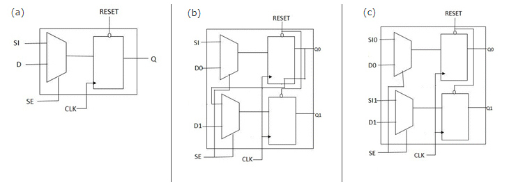
Multibit flops are used to optimize switching power generally in clock networks and also for improving area numbers. A group of 2 register bits can be implemented as a single 2-bit library register. Using following method, we have converted major single bit flops in multiple blocks to 2-bit MBITS to achieve significant improvements.
Requirements:
Clock, set and reset condition must be the same for single bit flop and 2-bit flop. For Scan enabled flops, we have to use one scan input and one scan output for each register bit. Single scan-in and scan-out is also possible using some additional logic inside multibit flops. Both types of MBIT scan register architectures are supported.

Multibit flip-flop Conversion:
There are multiple ways to convert single bit flops to multibit flops. We have found the following method efficient for our Networking ASICs.
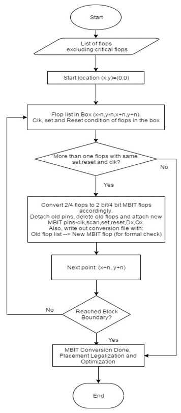
- List out the flops which are eligible for converting. Exclude user defined critical flops if given in the list.
- Take first flop in the list, which is closer to the block’s starting location. (0,0)
- Check nearby flops to combine:
- Get (x,y) and clk/set/reset info of the first flop.
- Find Multiple flops in box from starting point of the first flop: for example, for radius of 20um (all sides). First flop locx:40, locy:90. Box will be [20 70 60 110]
- Exclude flops which are not in conversion array.
- Exclude flops which are not having same clk/set/reset conditions.
- Let’s assume we found 5 registers nearby with all matching conditions that prevail. Find out the nearest 1 flop (for 2-bit) or 3 flops (for 4-bit) MBIT for register conversion. We have taken 2-bit conversion only for our blocks.
- Give names to the instances as: mbit_reg1_reg2 and dump it all to one list which will be useful for formal checks after conversion.
- Attach old clk/set/reset pins to mbit clk/set/reset pins. Attach D0/Q0 of mbit to reg1: D/Q and D1/Q1 of mbit to reg2: D/Q. Attach scan pins also as per mbit architecture: (single or multi scan pin configuration.)
- Delete old flops which have been already converted to MBITs.
- Revise step: 2-6 incrementally for all remaining flops.
- Incremental Placement legalization and optimization for all new flops.

Benefits of Multibit flops:
- Area reduction because of shared transistors and transistor level optimized layout: Area of Multibit cell is less than two single bit cells because of transistor level optimization of cell layout, which includes shared logic, power-supply and substrate-well.
- Total length of clock tree is reduced: This results in reduction of clock-tree buffers and clock-tree power. Clock-tree buffer level reduction improves overall balanced design skew.
CASE STUDY: Physical Design on TSMC’s 16nm FinFET for SDN Download Now
Disadvantages of Multibit flops:
- Concentrated congestion spots sometimes increase due to the combined logic of multiple flops placed in limited area. It can be solved through optimization techniques like Cell padding, partial placement blockages, max density, skip tracks, etc.
- Formal checks are complex after multibit conversion.
- QoR of complex designs sometime degrades, requiring more optimization iterations.
| Blocks | Complexity | Density |
Timing |
Shorts/DRC |
Dynamic Power Improvement after MBIT on | |||
| MBIT off | MBIT on | MBIT off | MBIT on | MBIT off | MBIT on | |||
| Case 1 | 50 Macros, 0.8M logic | 45% | 40% | -0.075/227 FEP | -0.046/146 FEP | 0/21 | 6/22 | 40% Reduction in clock network |
| Case 2 | 150 Macros, 1.5M logic | 55% | 48% | -0.150/500 FEP | -0.058/150 FEP | 100/250 | 37/130 | 35% reduction in clock network |
| Case 3 | 100 Macros, 1M logic | 42% | 40% | -0.010/1 FEP | -0.058/432 FEP | 252/856 | 8830/ 23666 | – |
Table 1: comparison table of some blocks taken from networking ASIC.
We have 10% blocks like Case 3 where MBIT on is having broken results of timing and DRC. Those 10% blocks are with MBIT off. Another 90% blocks have MBIT on and with conversion ratio of 90-95% to multibit flops, Blocks are closed for signoff with all checks passed.
Overall ASIC Power Improvement:
- Clock Power Reduction: 25%
- Data Power Reduction: 5%
- Leakage Power Reduction: 25%
What is MIMCAP?
Metal-Insulator-Metal (MIM) capacitors are parallel plate capacitors formed by two metal films. There is a thin insulating dielectric layer between Capacitor top metal- CTM and capacitor bottom metal- CBM layers. These MIM layers are made from Al, AlCu alloys, TiN, Ti, TaN, and Ta. While dielectric layers are made from silicon nitride or silicon oxide.
RELATED INFOGRAPHICS
Proven Tips for Right Time-to-Market at 16nm Lower Technology Node [Infographic]
Why MIMCAP is needed?
The geometry scaling has led to thinner interconnects and reduced metal width. Interconnect lengths were also increased along with switching at gigahertz speeds to meet complex ASIC design requirement. The device scaling has increased the density of integrated transistors on the semiconductor wafer (Silicon). There may be large current spikes due to simultaneous switching within short periods of time, which can cause the current resistance drop, voltage fluctuation and noise on the power supply network. These will affect reliability, speed and signal integrity. The addition of on-chip decoupling MIMCAP compensate voltage fluctuations by supplying charges to the power network. However, the capacitance must be large enough to meet the requirement.
MIMCAP Structure

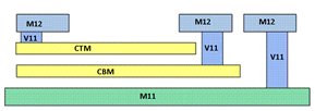
In 16nm project, the MIMCAP was placed between Metal 12 and Metal 11. A Metal-Insulator-Metal Capacitor (MIMCAP) uses a cut layer (V11) that connects a metal layer M12 to metal layer M11. The cut layer (V11) connects top layer metal layer M12 to intermediate layers CBM and CTM. The intermediate layers (CBM and CTM) are defined in the technology file with the MIMCAP function.
| Layer | Function | Mask |
| M12 | Metal | 42 |
| V11 | Cut | 61 |
| CTM | MIMCAP | 77 |
| CBM | MIMCAP | 88 |
| M11 | metal | 41 |
Table 2: Layer Function table for MIMCAP from Foundry.

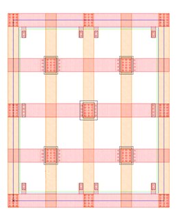
Above figure shows 4X4 MIMCAP of size 46×55 um^2.The cell cap is 42pF and Cap Density = 42700fF / (46.08*55.296 um^2) = 16.8 fF/um^2.
It is a cover cell. It has via11 obstruction in MIM region and M11 obstruction under MIM vias. It has no CTM/CBM shapes. Coupling to CTM/CBM seen only in extraction.
Where to Add?
MIMCAP cells are added to the blocks after power grid insertion. Decap cells are still required. MIMCAP doesn’t replace decaps, it rather adds to it. It is recommended to add these to places where there is little or no metal11 routing, since coupling to metal11 won’t be seen until extraction. It is recommended adding over high current density areas, such as TCAMs, high density or frequency logic areas, etc. There are placement rules regarding MIMCAP and die edge. Recommend >400u away from die edge.
Conclusion:
In our 16nm networking chip of 22*15 mm size with mentioned usage of MBIT flops and MIMCAPs, we got significant clock/data dynamic power improvements and extra 750pF decap with cost of extra manufacturing mask layer.
Are you looking for faster tape-out solutions across 16nm and below technology node? Let’s Connect


