To all the shutterbugs out there, do you ever stop and think for a moment how did those images in your smartphone camera or camcorder turn out so crisp and clear?
That too in conditions ranging from low light, indoors, against bright sunlight and sometimes, depending on your camera, even in pitch darkness.
Basically, there are several noise factors that degrade the quality of an image captured by camera e.g. real imperfections caused by the lens, color filter camera or the sensors.
To address them, a camera must embed what is known as image signal processing in the image processor, which is also referred to as an “image signal processing (ISP) pipeline” or a “video signal processing” pipeline.
eInfochips is doing pioneering work on cutting-edge IP camera products. In this blog series, I will share a developer’s perspective on how a modern camera works, starting with a description of the ISP pipeline.
Bonus Content : Get your free Whitepaper on Surveillance Camera – Market Research, Benchmarking and Go-to-Market Strategy
Basic Terminologies Used:
Raw Image:
This refers to minimally processed data from the image sensor. The raw image is so named because they have not been processed yet while containing all information necessary for further image processing.
YUV Image:
YUV data refer to the output of an ISP pipeline. It is a color space which encodes a color image, allowing reduced bandwidth for chrominance components. It contains one luminance and two chrominance components.
Effective pixels:
There are a large number of pixels in any given image. However, not all of them can be used in image creation. These are known as the “edge pixels” which happen to be ignored by the camera, but the data is still used by the pixels further away from the edge – the “effective pixels” are those that capture incoming light, and will end up in the final image.
Image Sensor:
Image sensors in a camera detect and convey the information that constitutes an image. A color image sensor uses what is known as the Bayer filter mosaic to provide a raw image.
Image Signal Processing:
Image signal processing (ISP) is a method used to convert an image into digital form while performing some operations on them, in order to get an enhanced image or to extract some useful information.
The two types of methods used for image processing are analog and digital image processing. Typical steps in ISP include importing the image, analyzing and manipulating it with data compression and enhancements to spot patterns that are not discernible to the naked eye. The final step involves converting the image to an output for further processing.
ISP Pipeline:
ISP pipeline refers to a dedicated piece of hardware which further converts RGB image to YUV image with several corrections needed to achieve better image quality.
Video Front End:
This refers to a part of a multimedia SoC (for example, Qualcomm Snapdragon 820) which is responsible for capturing image from the sensor and provide YUV data after necessary processing. VFE is normally clocked by PCLK (pixel clock) from the sensor.
Success Story: 4K Camera Design
Learn how eInfochips enabled a client to develope world’s first UltraHD 4K IP Camera.
Inside an Image Sensor:
Our basic understanding of image sensors can be summarized as:
“Light travels through a lens, the shutter opens, and a moment is preserved by capturing it on the camera’s sensor”.
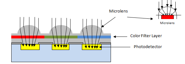
The basic building blocks of an image sensor are photodiodes which perform the conversion of light.

Figure 1: Principle of Image Sensor
As the camera’s sensor is photosensitive, when light photons are collected in the photosites (one photosite for each pixel), a tiny electrical charge is produced.
The incident light is directed by the microlens (a tiny lens placed over the pixel). The brighter the light, the more photons are collected, and a higher electrical charge is generated.
Different pixel photosites will register different electrical charges and, once the exposure is complete, each individual pixel photosite’s electrical charge must be measured and then turned into a digital value by an analog-to-digital converter.
There are a few different technologies used to manipulate those values. Two of the most popular types of sensors which use different technologies to measure these values are explained below.
Types of Image sensor modules
CCD (Charge-Coupled Device):
In CCD type of image sensor, when light strikes the chip, it is held as a small electrical charge in each photo sensor. The charges in the line of pixels nearest to the output amplifiers are amplified and converted to an output, followed by each line of pixels shifting its charges one line closer to the amplifier.
This process is then repeated by transporting the charge across the chip until all the lines of pixels have had their charge amplified and converted into an output.
An analog-to-digital converter (ADC) then turns each pixel’s value into a digital value by measuring the amount of charge at each photosite and converting that measurement to binary form.
CMOS (Complementary Metal Oxide Semiconductor):
A CMOS imaging chip is a type of image sensor that uses several transistors to amplify each pixel instead of a few CCD amplifiers and move the charge using more traditional wires. It uses red, green, and blue color filters and
It uses red, green, and blue color filters and passes data through metal wiring and onto photodiodes. Most modern sensors are of the CMOS variety.
As shown in above figure, the microlens which sits above the Bayer filter helps each pixel capture as much light as possible. The pixels do not sit precisely next to each other as there is a tiny gap between them.
Any light that falls into this gap is wasted light, and will not be used for the exposure. The microlens aims to eliminate this light waste by directing the light that falls between two pixels into one or other of them.
HANDPICKED RELATED CONTENT:
Check out second blog of this series: A Peek inside your Camera – II: Image Sensor Modules
How color image is produced:
Usually, the photodiodes employed in an image sensor are color-blind by nature, because they can only record shades of gray.
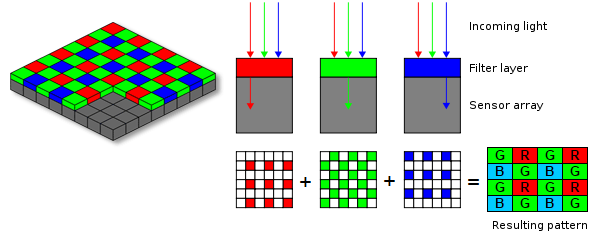
To get color into the picture, as shown in Figure 1, they are covered with a filter on top. This filter is usually a palette like red, green and blue (RGB) according to the pattern designated by the Bayer filter. The color image sensor uses Bayer filter to output raw Bayer image.
The color image sensor uses Bayer filter to output raw Bayer image.
Bayer Transformation:
The process to add colors in the image is known as Bayer transformation. Color filter array (CFA) is applied to the incoming raw data for arranging RGB color. An important aspect to understand in this whole process is the pattern of color filters.
An important aspect to understand in this whole process is the pattern of color filters. Usually, the pattern of color filters is arranged in such a way where half of the total number of pixels are green (G), while a quarter of the total number is assigned to both red (R) and blue (B), the reason is a human eye is more sensitive to green color.
When the image sensor is read line by line, the pixel sequence comes out as GRGRGR, etc., and then the alternate line sequence is BGBGBG, etc. as shown in below diagram.

Figure 2: Bayer Transformation
There are four possible ways such a pattern unfolds as seen in the following image.

Figure 3: Bayer filter patterns
From this color filter array pattern, the most popular patterns derived are RGGB, GRGB and RGBG which are a combination of RED and BLUE pixels.
The raw output produced from Bayer-filter cameras is referred to as a Bayer image. This image is then further processed using ISP pipeline to achieve quality pictures with all the necessary corrections applied.
Summary:
To summarize this blog, we have understood the internal specifics of image sensor processing and its basic principles, and how raw Bayer image is produced by applying Bayer filter.
In part 2 of this blog series, we will extensively discuss how this raw image is further processed to create a final YUV image. Stay tuned.
eInfochips has designed many award-winning high-resolution cameras, covering 4K, night vision, body worn, PTZ cameras etc.
They have been deployed in a wide range of applications from consumer devices to drone surveillance to perimeter security etc. To explore more about surveillance cameras in the market, check out our surveillance and camera benchmarking report.
Curious to know more about Camera Design?
Download free Camera Benchmarking Report. Time to Do Benchmarking for a 100% Success Rate


