To keep up the pace with Moore’s law, manufacturing technology nodes keep decreasing so much so that new issues of reliability, crosstalk, glitches, electromigration, and IR drop aware timing closures have been driving the design implementation methodologies. The need to partition the SoCs into manageable block sizes to be handled by EDA tools, exploit the compute resources, runtimes, and integration of these blocks back into the full-chip is a gigantic task. There are many integration issues seen at full-chip even though the standalone blocks are clean.
In this article, we will focus on one such case study to understand and share our learning that how a simple straight forward-looking block closure becomes vulnerable at full-chip once they are integrated into the top level. We faced a scenario where our block-level internal and interface timing were closed for all blocks. However, when we integrated all the clean blocks at the top level, one of the blocks failed in internal timing. There was one internal timing path from REG to SRAM which had hold violation. It’s an interesting learning of debugging and fixing. This paper majorly focuses on WHAT, WHY, and HOW to describe the entire learning process.
Problem Statement
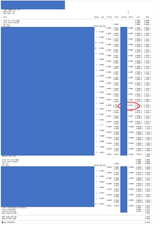
A standalone block with positive slack for internal REG to SRAM timing path fails to meet timing for the same path once the block is integrated at the full-chip. The path that was meeting by +7ps slack at block started violating at full-chip flat by -20ps slack.
Challenges
Our team was working on one of the multi-million gate SoCs and we had closed almost all the blocks in all metrics of physical verification and timing as well as reliability with acceptable quality.
The blocks were integrated at each netlist milestone, hierarchical timing runs were run regularly, and interface timing closure feedback to blocks was provided from time to time. This approach had given us high confidence on convergence and methodology that we were incorporating the block-level feedbacks into the full-chip and vice versa as well as flow/methodologies at every major milestone and we progressed well.
However, running full-chips flat is the only way to ensure that everything is fine and there are no outliers. But flat extraction and timing are computing and time-intensive, so the flat runs were kept intentionally limited. As luck would have it, we proved to be unlucky and the final run came up with one hold violation at the block level in full-chip context. The path was internal REG to SRAM violating by -20ps of slack.
We explored the possibility of waiving but since it was a hold violation, we decided not to risk but to fix the problem.
Brainstorming and Debugging
Here we go! Once we decided that it is a MUST FIX, it was time to do detailed brainstorming and debugging. The fixes are easy but identifying the problem and fixing it in the right location is the most difficult part.
We started comparing the full-chip timing report for the violating path and the same path from the timing report at the block level. Looking at every net, cell transitions, fanouts, capacitances, annotations, and crosstalk delta – we finally nailed it. The culprit was crosstalk at the block-level net.
At the block level -17p of crosstalk delta on the net was giving the timing slack of +7p that is marginally positive, but at the full-chip, the same net was generating -11p of the delta, reducing the downstream incremental delays of the cells, and hence making the capture path faster. This caused a hold violation with -20ps slack at the full-chip. A small difference of the crosstalk delta for the same net at the block-level and the full-chip level was causing the chip to fail.
Next, we decided how much margin we needed at the block level so that if we increased the positive slack at the block-level, we could gain by that amount at the full-chip.
Our block standalone had +7p of slack and the full-chip was violating by -20p. So logistically, we needed to increase the slack by 27ps OR more (27ps = 20p+7p) at block level to meet the full-chip path.
Block timing before fixes
Here is the excerpt of the timing report at the block level that shows that the timing is met with +7p of slack.

Full-chip timing before fixes
Here is the same report taken from full-chip that shows that the same path is failing by -20ps of slack.
Solution
Now we know WHAT was the problem, WHY it occurred, –and HOW to fix it. We explored the following options and finally chose one.
- First, we tried to see if there were any setup margins available on the downstream logic of SRAM since the path endpoint was SRAM. However, the downstream path from SRAM adds higher CK to Q delay. Any buffer addition was adding to the stage delay that was breaking the setup timing of the path in one or another scenario of multi-mode-multi-corner setup.
- We also checked setup margins at the pins of cells between the Start point and End point but no luck there.
- Since we were on the verge of full-chip closure, we were not too keen on disturbing the design too much by adding the cells to fix the crosstalk.
- The final option and the only way, we were left with was to try the metal fix, changing the layers to fix and impact minimal in the design. This also looked more feasible because the memory channel was densely populated with the cells and adding anything there would lead to disturbing other neighboring cells.
- We looked at the layout, highlighted the net with the crosstalk, and reported each layer segment in which the net was routed.
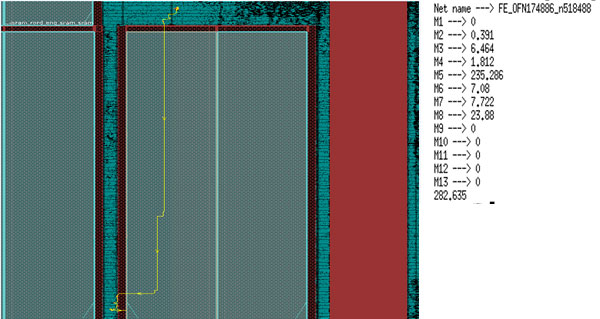
The net was routed for a maximum length of 235u in only the M5 layer that was going over SRAM. We converted this M5 to M3 in the lower layer. We reduced the M5 segment to < 10u and increased the M3 routing segment from <10u to ~230u keeping the overall net length nearly the same as earlier.
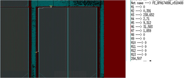
This solution worked well for us. After making this change from M5 to M3, we ran block-level timing and saw that the same path now MET with +35p.
Block Timing after M5 to M3 routing change
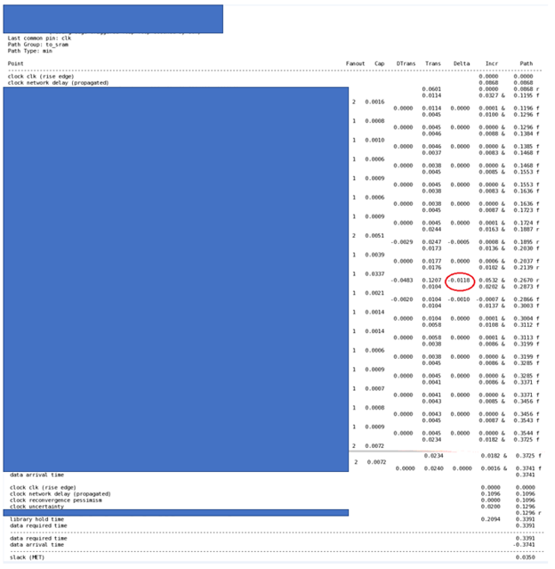
We needed 27p of margin (20p violation at full-chip + 7p of slack at block) at the block level so that we could meet at full-chip and with this solution, we had 28p of margin increased at the block-level (28p=35p postfix – 7p prefix). The required margin we got for this effort matching with the requirement was merely a coincidence, if this would not have matched, we would have tried to look for other options. The goal was to increase the positive margin at block level so that it meets timing at the full-chip. We re-ran full-chip flat timing again and ensured that what we tried on the block was reflected at full-chip and this was a happy ending! The silicon is already part of the working product and is available in the market.
Conclusion
Crosstalk is a major problem in the timing closure of deep sub-micron technologies. On many occasions, we came across a situation where the timing paths setup and hold both became critical. This means that we can not fix setup without braking hold and viseversa. When we find such paths, we are too late in the cycle and constrained by schedules, metal-only changes, programmable ECO filler cells, congested areas, routing restrictions, and runtimes.
It is always better to apply certain solutions upfront in the PNR flow like limiting the net length, shielding critical nets, wire spreading techniques to avoid crosstalk as much as possible. However, there will be always some corner cases due to mismatch in timing windows, slew, derates, noise, and library modelings. These are the challenges that make a physical design engineer’s work interesting and make it a learning process.
eInfochips – An Arrow company has been working on SoC chips and IP development for more than 15 years. While working for many customer projects in the field such as ethernet switches, data center storage, cloud computing, and consumer application, eInfochips has developed many proofs-of-concept in physical design implementation flow to help achieve faster time to market and bug-free designs for its customers. To know more about our expertise please contact our experts today.