What is LVS?
In ASIC physical implementation, once layout is generated, it must follow all the design rules for successful manufacturing and must match the schematic of the required design. To ensure this in physical verification, Design Rule Check (DRC) is carried out to check whether the layout follows the rules for fault-less manufacturing or not. This DRC checks provide good manufacturing yield and prevents faults during manufacturing, however it does not ensure the correctness of the layout. It needs to be ensured that, the physical implementation of the design is the same as the schematics of the design. For this, the electrical circuit of layout netlist is compared against the schematic netlist, which is known as Layout versus Schematic (LVS).
Here IC Validator and IC Compiler-II (SYNOPSYS) tools are used for LVS runs and PnR.
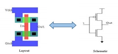
As shown in the above figure, LVS is a comparison between layout, which is represented by GDS and schematic that is generated by the tool using verilog netlist.
Input files for LVS in ICV tool are listed below:
- GDS (layout stream file): It is used by the LVS tool to generate layout netlist by extraction, which is used for LVS comparison.
- Schematic netlist: It is used as a source netlist for LVS comparison.
- Rule deck file: Rule deck file consists of required instructions and files to guide tool for performing LVS. This rule deck file also contains a layer definition, which is useful for extraction.
- Equivalence file: It is used by the tool for ICV LVS comparison and it consists of cell pairs, which is made-up of one from the layout netlist and another from the schematic netlist.
RELATED BLOG
LVS Flow
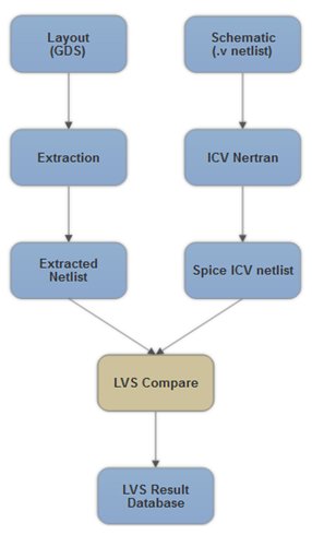
LVS flow is mainly consisting of extraction and comparison of layout netlist and schematic netlist. LVS flow is depicted in the figure-2. ICV has nettran utility for translation of input verilog netlist to ICV schematic netlist, which is further useful for comparison purpose. All devices and connections between them are extracted from GDS in the layout extraction step. The tool also generates an equivalence point file after the extraction for comparison of layout and schematic. This equivalence file is useful for comparison. In comparison step, extracted netlist is compared with schematic netlist and the tool gives clean result, if both the netlists match completely and if not, the tool generates error reports. In comparison step, tool does the comparison in the following way: Tool compares the number of devices in schematic and in layout, the number of nets in schematic and in layout, types of device in schematic and in layout, and then generates the result reports. Error report contains a list of incorrect devices, incorrect nets, which is useful to debug the LVS issue.
Get silicon tape-out solutions across lower technology nodes from 180nm to 16nm,7nm,5nm and below
Common LVS issues and their debug
- Open
- Shorts
- Missing components
- Missing global net connect
Open: Shapes of the nets having the same layout text on them are not intersecting or touching causes opens in design. Opens in the design are responsible for floating connections in the design. This floating connection will cause major defects in chips (ASIC/FPGA). So, it is very important to find opens in the design. Running open finding utility of PnR tool before running LVS, is helpful in the early design phase.
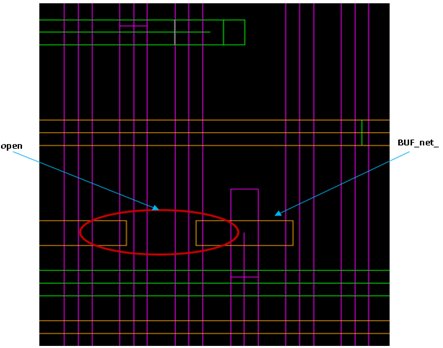
The example below is showing detection of the open in the design by LVS tool. Reports generated by the tool describes the open in the design as shown in the following snippet of the tool report.
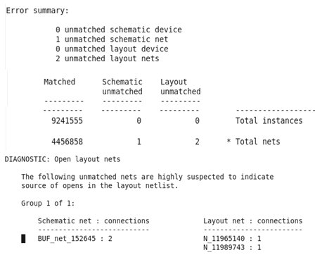
Error summary shows the summary of detected errors with their counts. For open, extractor extracts the open net as two different nets, so the number of nets in the layout is greater than the number of nets in the schematic, as shown in the report. The report, shows the number of nets in the layout with corresponding schematic. The schematic net BUF_net_152645, which is represented by two nets N_11965140 and N_11989743 in layout (because of the open), as mentioned in the report.
This type of issue can be solved by connecting layout shapes of single net that is left open.
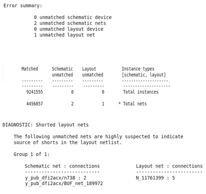
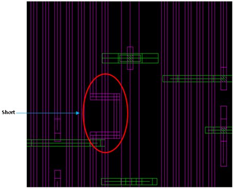
Short: If layers in layout having different layout text on them are overlapping or intersecting, it will result in short in the design. Presence of the short in design will cause chip failure. It is important to find shorts present in design by running PnR shorts finding utility or by running LVS. The following example shows, how the short is reported by the tool after running the LVS.
Looking for Physical Verification Assistance? We are here to help!
When the short occurs in the design, the extractor will extract shorted nets as a single net, so there is only one layout corresponding net for two nets in the schematic, as mentioned in the report. N738 and BUF_net_189972 are shorted nets.
Short can be resolved by properly rerouting the net.
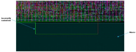
Internal shorts with Macros: In a physical design, due to the complexity of the design or due to incorrect settings, it can happen that the PnR tool routes nets in a way that creates short with the internal geometries of the macros. It can also happen if routing blockage is missing in LEF of the macro. Sometimes while doing manual custom routing, short is created between custom route and the internal routing of the macro. This short is not easily reported in the PnR tool environment. When we merge the GDS of the hard macro with the top-level block, the short is visible in the GDS. This short can be debugged using VUE utility of ICV. Below is a snippet that shows how a signal net is incorrectly routed over the hard macro. The layer is blocked over the macro, as internal geometries of the hard macro is present. This net will cause a short with the internal geometries of the macro.
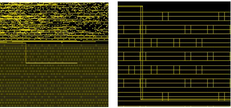
Below is the snippet from the merged GDS, which clearly shows the short.
Generated report is similar as shown for the short report. Snippet for this example is as follows.

PG short with signal net: When there is a PG short in the design, it is very difficult to identify it. PG short can be a short between a power net and a ground net or it can be a short between a power/ground net and a signal net. When a PG net is shorting with fairly long signal net and since the PG net is connected to so many devices, it is very difficult to pin-point a short location. To debug this issue, there is a way in ICV to add a text on the signal net which is shorting with PG net.
Following is an example of adding a text over the signal net. This net name can be easily figured out from the LVS error report. Take any location where the shorting signal net exists (take any layer) and put a text of any tag name over it, at a location defined by origin value in the below command.
create_shape -shape_type text -layer <layer_name> -origin <{llx lly}> -height 1 -orientation R0 -justification LB -text “<any_text_name>”
Below is an example of how to debug PG short with any signal net using text addition.
Due to incorrect metal fill and manual routing changes, a short was created between VSS net and one of the signal net as shown in the figure below.
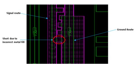
It was very difficult to figure out the short location as the signal net itself was very long. On the signal net, a text layer was created using the command shown above and LVS was rerun. Now, the short between VSS and text was easily visible in the LVS short finder, and the snapshot above shows the error highlighted using VUE database of ICV.
Missing components
If some of the spice file or GDS file is missing while merging database, it shows missing components error. For example: if you have cell ABC used in the design, but not defined in GDS list or spice list to be used for LVS flow, it can cause missing components error. Either the list needs to be modified or ABC cell needs to be excluded from the LVS comparison (this depends on the functionality of the cell, only physical cells may be excluded in the comparison).
Missing global net connect
If PG pins of the cells is not connected to any power/ground net using connect_pg_net commands, it causes device mismatches and LVS errors for most of the design. For example, even if the standard cell PG pin name is VDD, tool does not connect it to VDD net of design. We need to use below command to connect such pins.
connect_pg_net -net VDD [get_pins -hierarchical */VDD]
Conclusion
LVS is useful technique to verify the correctness of the physical implementation of the netlist. open, shorts, missing components, and missing global net connect are potential issues that can affect the functionality of design and may not be detected at early implementation stage, so LVS is useful to report these issues in design. Once these issues are reported by Physical verification tool, it can be solved by various techniques as discussed in this article.
Chirag Rajput, Nilay Mehta & Chirag Maniya


