Over the years, we have seen a wide range of advancements in semiconductor design services. The Semiconductor Industry Association (SIA) announced that the global semiconductor industry posted sales of $468.8 billion in 2018 – the industry’s highest-ever annual total and an increase of 13.7 percent over the 2017 sales.
As the demand for semiconductor technology node design services continues to increase and the industry witnesses a broader range of new technology innovations, we can clearly see a move toward lower geometries (7nm, 10nm, 12nm, 16nm, etc.). The key drivers behind this trend are benefits in terms of the power, area, plus various other features that become possible with lower geometries.
The proliferation of lower geometry design has fuelled business in a number of areas, especially in the sectors of mobility, communication, IoT, cloud, AI for hardware platforms (ASIC, FPGA, boards).
Delivering a lower technology node design project on time is important in today’s dynamic and competitive market. However, there are many unknowns at lower geometry which impacts on project/product scheduled delivery. By keeping in mind the below elements, it is possible to ensure on-time delivery at lower technology nodes.
1. Lower technology node’s cost modeling
A chip design leader provides the required strong technical leadership and has the overall responsibility for the integrated circuit design.

Image Source: ExtremeTech.com
For lower geometry design, VLSI engineers need to define the activities from specification-to-silicon design, sequence them in the right order, estimate the resources needed and estimate the time required to complete the tasks. At the same time, they need to focus on the reduction of the total system cost while also satisfying specific service requirements. Following are the actions that engineers can take for cost optimization:
- Use multiple patterning
- Use suitable design-for-testability (DFT) techniques
- Leverage mask making, interconnects and process control
DOWNLOAD CASE STUDY
Physical Design of a 7nm based Superfast Programmable Ethernet Switch ASIC
On different layout methods because node scaling down is not cost-economic anymore. For continuous performance improvement along with cost control, some companies are now pursuing a monolithic 3D ICs rather than a conventional planar implementation, as this can provide 30% power savings, 40% performance boost, and cut the cost by 5-10% without changing over to a new node.
2. Advanced data analytics for smart chip manufacturing
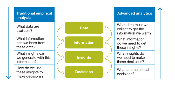
In the semiconductor chip manufacturing process, a large volume of data is generated on the fab floor. Over the years, the quantity of this data has continued to grow exponentially with each new technology node dimension. Engineers have played instrumental roles in generating and analyzing data with the aim of improving predictive maintenance and yield, improving R&D, enhancing product efficiency and more.

Image Source: McKinsey & Company
Applying advanced analytics in chip manufacturing can help to improve the quality or performance of individual components, cut-down test time for quality assurance, boost throughput, increase equipment availability, and reduce operating costs.
3. Efficient Supply Chain Management
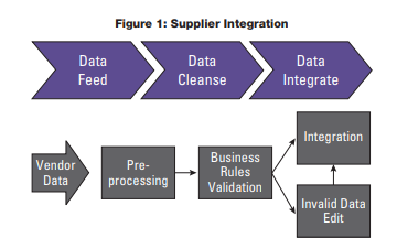
As new technology is often released faster than the R&D timeline, everyone in the chip-making industry is facing a problem in IC supply chain management. The big question is: how to improve efficiency and profitability in this scenario.

Image Source: Tensoft.com
The answer is faster decision making and efficient integration of various suppliers, requirements of clients, distribution centers, warehouses, and stores so that merchandise is produced with end-to-end supply chain visibility and distributed in the right quantities, at right time to the right location to minimize total system cost.
How to deliver on time at Lower Technology Nodes? #LowerTechnologyNode #TimeToMarket #ProductEngineering #SupplyChain #Cost #ChipDesign via @einfochipsltd
4. Process for timely delivery
Improved delivery to the customer is a core part of the semiconductor design services. It includes setting-up order capturing to work with orders at runtime, cloud computing optimization, logistics, and the transfer the end-product to a customer – while keeping them up-to-date with every required information at each stage. Planning the complete flow ensures that no critical deadlines for the project are missed.
In order to overcome delays, semiconductor design companies can:
- Minimize the use of custom flows and shift towards place & route flows for better physical data-path capabilities.
- Set and adhere to quick response time to the client’s requirements and change requests.
- Get real-time information from spec to silicon availability in terms of the semiconductor design flow, location, reservation, and quantity.
- Ensure collaborative communication between teams working on the project.
- Focus on criticality analysis – reducing the risk of functional failures of the design to prevent business stoppers.
- Gain utilization expertise in multiple tools for managing the project.
- Adopt better technologies (TSMC, GF, UMC, Samsung), better methodology (Low power consumption and high-speed performance), better tools (Innovus, Synopsys, ICC2, Primetime, ICV).
How is eInfochips positioned to serve the Market?
Whether you want to design innovative products faster, optimize R&D costs, improve time to market, enhance operational efficiency or maximize the return on investment (ROI), eInfochips (an Arrow Company) is the right design partner.
eInfochips has worked with many top global companies to contribute over 500 product designs, with more than 40 million deployments around the world. eInfochips has a large pool of engineers who possess specialization in PES services, with a focus on in-depth R&D and new product development.
In order to deliver the product at short time-to-market, eInfochips provides ASIC, FPGA and SoC design services based on standard interface protocols. It includes:
- Sign-off services in the front end (RTL design, Verification) and backend (Physical design and DFT-DFM)
- Turnkey design services covering Netlist to GDSII and design layout
- Use of Reusable IPs and framework that assist the company in short product development time and cost for faster and right time-to-market


