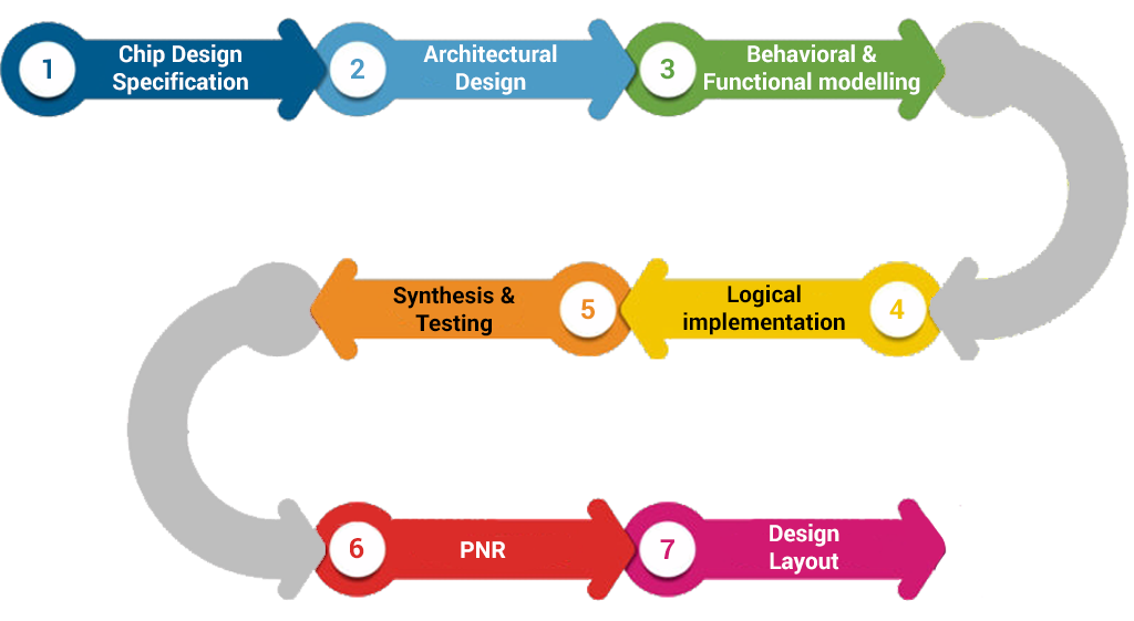
Today, ASIC design flow is a very mature process in silicon turnkey design. The ASIC design flow and its various steps in VLSI engineering that we describe below are based on best practices and proven methodologies in ASIC chip designs. This blog attempts to explain different steps in the ASIC design flow, starting from ASIC design concept and moving from specifications to benefits.
Why to adopt the ASIC design flow?

To ensure successful ASIC design, engineers must follow a proven ASIC design flow which is based on a good understanding of ASIC specifications, requirements, low power design and performance, with a focus on meeting the goal of right time to market. Every stage of ASIC design cycle has EDA tools that can help to implement ASIC design with ease.
How does the ASIC design cycle work?
In order to fulfill futuristic demands of chip design, changes are required in design tools, methodologies, and software/hardware capabilities. For those changes, ASIC design flow adopted by engineers for efficient structured ASIC chip architecture and focus on its design functionalities
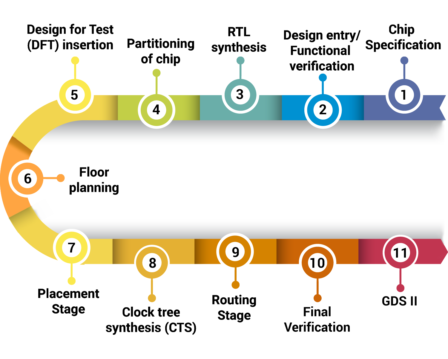
ASIC design flow is a mature and silicon-proven IC design process which includes various steps like design conceptualization, chip optimization, logical/physical implementation, and design validation and verification. Let’s have an overview of each of the steps involved in the process.

Step 1. Chip Specification
This is the stage at which the engineer defines features, microarchitecture, functionalities (hardware/software interface), specifications (Time, Area, Power, Speed) with design guidelines of ASIC. Two different teams are involved at this juncture:
- Design team: Generates RTL code.
- Verification team: Generates test bench.
Step 2. Design Entry / Functional Verification
Functional verification confirms the functionality and logical behavior of the circuit by simulation on a design entry level. This is the stage where the design team and verification team come into the cycle where they generate RTL code using test-benches. This is known as behavioral simulation.
In this simulation, once the RTL code (RTL code is a set of code that checks whether the RTL implementation meets the design verification) is done in HDL, a lot of code coverage metrics proposed for HDL. Engineers aim to verify correctness of the code with the help of test vectors and trying to achieve it by 95% coverage test. This code coverage includes statement coverage, expression coverage, branch coverage, and toggle coverage.
There are two types of simulation tools:
- Functional simulation tools: After the testbench and design code, functional simulation verifies logical behavior and its implementation based on design entry.
- Timing simulation tools: Verifies that circuit design meets the timing requirements and confirms the design is free of circuit signal delays.
Step 3. RTL block synthesis / RTL Function

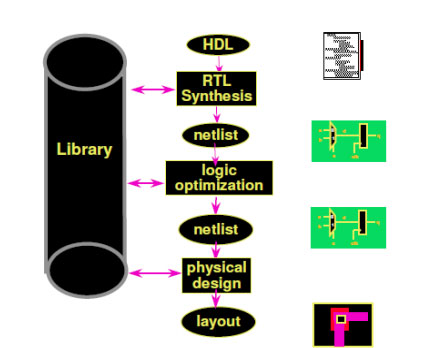
Once the RTL code and testbench are generated, the RTL team works on RTL description – they translate the RTL code into a gate-level netlist using a logical synthesis tool that meets required timing constraints. Thereafter, a synthesized database of the ASIC design is created in the system. When timing constraints are met with the logic synthesis, the design proceeds to the design for testability (DFT) techniques.
Looking for FPGA to ASIC conversion with Zero nre?
Step 4. Chip Partitioning
This is the stage wherein the engineer follows the ASIC design layout requirement and specification to create its structure using EDA tools and proven methodologies. This design structure is going to be verified with the help of HLL programming languages like C++ or System C.
After understanding the design specifications, the engineers partition the entire ASIC into multiple functional blocks (hierarchical modules), while keeping in mind ASIC’s best performance, technical feasibility, and resource allocation in terms of area, power, cost and time. Once all the functional blocks are implemented in the architectural document, the engineers need to brainstorm ASIC design partitioning by reusing IPs from previous projects and procuring them from other parties.
Step 5. Design for Test (DFT) Insertion
With the ongoing trend of lower technology nodes, there is an increase in system-on-chip variations like size, threshold voltage and wire resistance. Due to these factors, new models and techniques are introduced to high-quality testing.
ASIC design is complex enough at different stages of the design cycle. Telling the customers that the chips have fault when you are already at the production stage is embarrassing and disruptive. It’s a situation that no engineering team wants to be in. In order to overcome this situation, design for test is introduced with a list of techniques:
- Scan path insertion: A methodology of linking all registers elements into one long shift register (scan path). This can help to check small parts of design instead of the whole design in one go.
- Memory BIST (built-in Self-Test): In the lower technology node, chip memory requires lower area and fast access time. MBIST is a device which is used to check RAMs. It is a comprehensive solution to memory testing errors and self-repair proficiencies.
- ATPG (automatic test pattern generation): ATPG is a method of creating test vectors / sequential input patterns to check the design for faults generated within various elements of a circuit.
Step 6. Floor Planning (blueprint your chip)
After, DFT, the physical implementation process is to be followed. In physical design, the first step in RTL-to-GDSII design is floorplanning. It is the process of placing blocks in the chip. It includes: block placement, design portioning, pin placement, and power optimization.
Floorplan determines the size of the chip, places the gates and connects them with wires. While connecting, engineers take care of wire length, and functionality which will ensure signals will not interfere with nearby elements. In the end, simulate the final floor plan with post-layout verification process.
A good floorplanning exercise should come across and take care of the below points; otherwise, the life of IC and its cost will blow out:
- Minimize the total chip area
- Make routing phase easy (routable)
- Improve signal delays
Step 7. Placement
Placement is the process of placing standard cells in row. A poor placement requires larger area and also degrades performance. Various factors, like the timing requirement, the net lengths and hence the connections of cells, power dissipation should be taken care. It removes timing violation.
Step 8. Clock tree synthesis
Clock tree synthesis is a process of building the clock tree and meeting the defined timing, area and power requirements. It helps in providing the clock connection to the clock pin of a sequential element in the required time and area, with low power consumption.
In order to avoid high power consumption, increase in delays and a huge number of transitions, certain structures can be used for optimizing CTS structure such as Mesh Structure, H-Tree Structure, X-Tree Structure, Fishbone Structure and Hybrid structure.
With the help of these structures, each flop in the clock tree gets the clock connection. During the optimization, tools insert the buffer to build the CTS structure. Different clock structures will build the clock tree with a minimum buffer insertion and lower power consumption of chips.
For more details on CTS Challenges, Solutions and benefits,
Step 9. Routing
- Global Routing: Calculates estimated values for each net by the delays of fan-out of wire. Global routing is mainly divided into line routing and maze routing.
- Detailed Routing: In detailed routing, the actual delays of wire is calculated by various optimization methods like timing optimization, clock tree synthesis, etc.
As we are moving towards a lower technology node, engineers face complex design challenges with the need for implanting millions of gates in a small area. In order to make this ASIC design routable, placement density range needs to be followed for better QoR. Placement density analysis is an important parameter to get better outcomes with less number of iterations.
Step 10. Final Verification (Physical Verification and Timing)
After routing, ASIC design layout undergoes three steps of physical verification, known as signoff checks. This stage helps to check whether the layout working the way it was designed to. The following checks are followed to avoid any errors just before the tapeout:
- Layout versus schematic(LVS) is a process of checking that the geometry/layout matches the schematic/netlist.
- Design rule checks(DRC) is the process of checking that the geometry in the GDS file follows the rules given by the foundry.
- Logical equivalence checks(LVC) is the process of equivalence check between pre and post design layout.
Step 11. GDS II – Graphical Data Stream Information Interchange
In the last stage of the tapeout, the engineer performs wafer processing, packaging, testing, verification and delivery to the physical IC. GDSII is the file produced and used by the semiconductor foundries to fabricate the silicon and handled to client.
Conclusion
In the domain of VLSI engineering services, the mastery of the ASIC design flow stands as a cornerstone for achieving success. This concise guide has meticulously unraveled the intricate steps and methodologies integral to the development of Application-Specific Integrated Circuits (ASICs). From the initial design specifications to the final stages of physical implementation, it has diligently navigated through each phase, accentuating the critical roles of synthesis, verification, and validation.
Recent trends in ASIC design have ushered in remarkable advancements. Notably, the infusion of artificial intelligence and machine learning algorithms into the design process has revolutionized power management, leading to superior performance optimization. Additionally, the paramount concern surrounding hardware security has driven the integration of robust security features into ASICs, fortifying them against vulnerabilities and potential cyberattacks.
Moreover, the adoption of advanced process nodes like 7nm and 5nm has ushered in an era of increased transistor density, facilitating the development of more intricate and power-efficient ASICs. These smaller process nodes have also empowered the seamless integration of analog and digital components, enriching the overall functionality of system-on-chip (SoC) solutions.
In an ever-advancing technological landscape, this guide equips VLSI engineers with invaluable insights and tools, allowing them to adeptly navigate the intricacies of ASIC design. By embracing these recent trends and harnessing the latest technological innovations, ASIC designers are poised to continuously push the boundaries of what can be achieved in the dynamic realm of VLSI engineering services.
eInfochips has contributed to over 500 product designs for top global companies, with more than 40 million deployed around the world. As a leading ASIC design and verification service provider, eInfochips has brought together IP cores, verification IP and design and verification expertise. If you are looking for low power ASIC design assistance, we are here to help!


