The intent of this paper is to explain the varied kinds of DRCs (Design Rule Checks) that are encountered in the Physical Design flow. This paper will discuss the Metal DRC violations (7nm Technology) generally seen at the block level and outline the practical approach to fix them.
I. Introduction
Most of the VLSI engineers are aware of DRC and appreciate the need for a DRC cleaned database. This paper will give a brief idea about the different types of DRC violations, the reasons for their occurrence in the physical design, and the heuristic approach to fix it. We will also look at the Design Rule Checks proposed by the foundries (for example: TSMC, Intel, Samsung, etc.) and explore how they are targeted for the specific technology node (e.g. 28nm,16nm, 7nm).
The main objective of the Design Rule Check is to achieve reliability in the design and to improve the gross yield of the die. All the rules, provided by the foundry, are fed as an input to the Physical Verification Tool in the form of verification rule file (Rule deck file for Physical Verification Tool). If any of the rules are violated, the DRC will be reflected in the design.
II. Classification of DRCs
The DRCs are broadly classified as the Base Layer DRC and the Metal Layer DRC. The below figure depicts this classification.
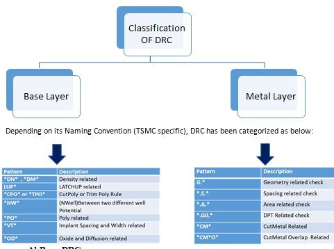
A] Base Layer DRC
The DRCs – which are associated with FEOL (Front End of Line) Process include Nwell, N+, P+ implant layers, poly, Oxide Diffusion, etc. – are referred to as Base Layer DRC. The fixation of these DRCs demands the alteration of FEOL layers. The general practice followed by physical designers is to fix these violations before the floorplan gets frozen or before the sign-off phase of the design cycle.
In the course of time, as the technology gets updated, the APR flow is developed to address the Base DRC in an augmentative way in order to avoid hitches in subsequent PnR/Sign Off stages of the physical design flow. Some of the DRCs can vary depending on DFM (Design for Manufacturability) practices followed by the different foundries.
Some of the Causes for Base Violations are:
- Missing Endcap/WellTap/Decaps/Filler cells
- Incorrect filler placement
- Incorrect filler addition
- Overlap issue or issue in the Internal Structure of the particular memory down model (Hard Macro/IP)
- Memory not on grid
- Orientation issue
- Input gate integrity problem
- Legalization issue
- Abutment requirement between two Memories is not met (Memory Spacing Rule varies in accordance to technology and foundry)
B] Metal DRC
The DRC associated with the BEOL (Back End of Line) Process are those that include interconnects or metal layers which are plugged with FEOL and external devices. The Cut Metal/Trim Metal DRCs are newly introduced in 7nm technology node. The Cut Metal is the new layer, which is introduced in order to minimize the EOL (End of Line) spacing, MAR (Min Area) violations, and Via Enclosure rule.
If you wish to download a copy of our whitepaper: Physical Design of a 7nm based Superfast Programmable Ethernet Switch ASIC
Benefits of Cut Metal Layer:
- Helps to maintain the shorter standard cell height (CM1A and CM1B) [Refer Fig c for a better understanding].
- It helps to reduce the distance (Left and Right) between the two standard cells due to CM2 [Refer Fig c for a better understanding].
- More M1 Routing resources availability.
- The Cut Metal helps for EOL (shrinking the end-to end-spacing) and MAR and Enclosure violations [Refer Figs a and Fig b].


III. Some Real Scenarios of Metal DRC Violations in 7nm
Here we discuss the techniques to fix the DRC violations seen in the 7nm ASIC Designs.
A.CM1A.S.3.1

A.1) With CM1A DRC
Here, the trapezoid marker denotes the error prompted at vertical metal layer (M1). The error is due to the absence of minimum spacing between the metal track and the Cut Metal present between the two vias (VIA12).

A.2) With CM1A DRC fixed
To solve this, we simply shifted the via (VIA12) tapping from its initial location in the downward direction. As shown in the figure, the highlighted track is the re-routed track, taken from vertical metal layer one (M1) in blue color to horizontal metal layer two (M2) in yellow color
B. M4.A.1

B.1) With M4.A.1 DRC
This DRC simply depicts the minimum area of the horizontal metal track four (M4) shown in green color, which is less than 0.015 microns2.

B.2) With M4.A.1 DRC fixed
To solve this, we have extended the horizontal metal layer four (M4) track. As shown in the figure, the re-routed track is taken from vertical metal layer three M3 in red to horizontal metal layer four (M4) in green.
C. VIA2.S.20

C.1) With VIA2.S.20 DRC
In here, DRC popped up due to the violation of minimum spacing between via of horizontal signal metal track layer two (M2) in yellow color with the via of the power tracks in the same layer. In the figure, the center mark is the signal track and at the corners of the triangle, there are two power tracks vias.

C.2) With VIA2.S.20 DRC fixed
This DRC was solved by re-routing the track away from the power vias. As shown in the figure, the highlighted tracks with zig-zag routing represent one of the possible solutions to eliminate this DRC.
D. M3.CS.1.1.6:CA

D.1) With M3.CS.1.1.6:CA DRC
The Cut Metal vertical layer three (M3) in red violates the minimum the spacing with the internal layer of the memory IP shown in blue color.

D.2) With M3.CS.1.1.6:CA DRC fixed
To solve this type, we re-routed the vertical metal layer three (M3) through horizontal metal layer two (M2) in yellow color.
E. M1 Enclosure DRC

The M1 Enclosure DRC can pop up in Calibre by the name H240*M1.EN*. It shows the DRC on M1 VIA internal to cell pin. This is due to the addition of patch measured as 0.028u which is lesser than the limit (<= 0.037u)

In order to fix the DRC, we can extend the patch to exceed the limit of 0.037u
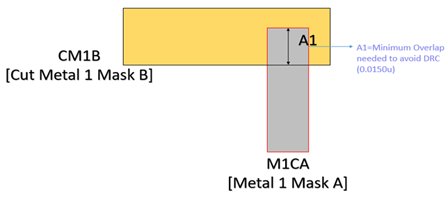
F. Cut Metal Overlap DRC

The Cut Metal Overlap DRC is tagged with the name CM1B.O.*. It is due to the overlapping of CutMetalM1 of Mask 2 or (Mask B) and the M1 of Mask 1 or (Mask A).

The vertical overlap between M1(MaskA) and CM1(MaskB) in this case is 0.008u. Just by extending the Patch by length greater than >=0.0150u, the DRC can be fixed.
See below diagram for detailed understanding:
G. Cut Metal Spacing DRC rules

This DRC is popped under the name CM2*S*
As in above figure, the Cut Metal for Mask 2 Layer M2 is present between two nets: netA and netB.
Cut Metal2 is giving spacing violation with NetC and NetD of Metal2.

By rerouting the small portion of NetC and NetD this Cut Metal spacing DRC can be solved.
IV. Conclusion
The successful tapeout of ASIC chips requires the DRC rules to be met for the better DFM yields. By using the methods explained in this paper, the different DRC violations related to the technology node 7nm can be addressed.
Some of the practical approaches we discussed in the paper can help in early closure of the design, and also help to reduce the number of iterations required at the sign-off stage. The end result is faster tapeout of the ASIC.
Get physical design services for 7nm technology node design?