The ‘Semiconductor era’ started in 1960 with the invention of the integrated circuit. In an integrated circuit, all the active-passive components and their interconnection are integrated on a single silicon wafer, offering numerous advantages in terms of portability, functionality, power, and performance. The VLSI industry is following Moore’s law for many decades, which says, “the number of transistors on a chip becomes double approximately every two years”. To get the benefits of a scaled-down transistor, VLSI industry is continuously improving transistor structure and material, manufacturing techniques, and tools for designing IC. Various techniques, which have been adopted for transistors so far, include high-K dielectric, metal gate, strained silicon, double patterning, controlling channel from more than one side, silicon on insulator and many more techniques. Some of these techniques are discussed in ‘A Review Paper on CMOS, SOI and FinFET Technology
Nowadays, the demand of the internet of things, autonomous vehicles, machine learning, artificial intelligence, and internet traffic is growing exponentially, which acts as a driving force for scaling down transistor below the existing 7nm node for higher performance. However, there are several challenges of scaling down a transistor size.
Issues with Sub-Micron Technology
Every time we scale down a transistor size, a new technology node is generated. We have seen transistor sizes such as 28nm, 16nm, etc. Scaling down a transistor enables faster switching, higher density, low power consumption, lower cost per transistor, and numerous other gains. The CMOS (complementary metal-oxide-semiconductor) transistor base IC technology performs well up to 28nm node. However, the short channel effects become uncontrollable if we shrink down CMOS transistor below 28 nm. Below this node, a horizontal electric field generated by drain-source supply tries to govern the channel. As a result, the gate is unable to control leakage paths, which are far from the gate.
16nm/7nm Transistor Technology: FinFet and FD-SOI
The VLSI industry has adopted FinFET and SOI transistor for 16nm and 7nm nodes, as both the structures are able to prevent the leakage issue at these nodes. The main objective of both the structures is to maximize gate-to-channel capacitance and minimize drain-to-channel capacitance. In both transistor structures, the channel thickness scaling is introduced as the new scaling parameter. As the channel thickness is reduced, there are no paths, which are far from the gate area. Thus, gates have a good control over the channel, which eliminates short channel effects.
[forminator_poll id=”8861″]
In Silicon-on-Insulator (SOI) transistor, a buried oxide layer is used, which isolates the body from the substrate shown in Figure 1(a).Owing to the BOX layer, drain-source parasitic junction capacitances are reduced, which results in faster switching. The main challenge with the SOI transistor is that it is difficult to manufacture a thin silicon layer on the wafer.

FinFET, which is also called as tri-gate controls channel is shown from three sides in Figure 1(b). There is a thin vertical Si-body, which looks like a back fin of fish wrapped by the gate structure. A width of the channel is almost two times Fin height. Thus, to get higher driving strength, a multi-Fin structure is used. One of the gains with FinFET is higher driving current. The main challenge with FinFET is the complex manufacturing process.
Challenges with Technology Node below 5nm: What Next?
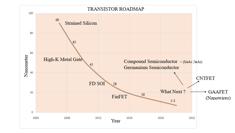
Reducing the body thickness results into lower mobility as surface roughness scattering increases. Since FinFET is a 3-D structure, it is less efficient in terms of thermal dissipation. Also, if we scale down the FinFET transistor size further, say below 7nm, the leakage issue becomes dominant again. Consequently, many other problems come into consideration like self-heating, threshold flattening, etc. These concerns lead to research on other possible transistor structures and replacing existing materials with new effective materials.
According to the ITRS roadmap (International Technology Roadmap for Semiconductors), the next technology nodes are 5nm, 3nm, 2.5nm, and 1.5nm. Many different types of research and studies are going on in VLSI industry and academia for potential solutions to deal with these future lower technology nodes. Here we discuss some promising solutions like carbon nanotube FET, GAA transistor structure, and compound semiconductor for future technology nodes.

CNTFET – Carbon Nano Tube FET
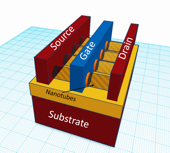
CNT (Carbon Nanotube) showcases a new class of semiconductor material that consists of a single sheet of carbon atoms rolled up to form a tubular structure. CNTFET is a field-effect transistor (FET) that uses semiconducting CNT as a channel material between the two metal electrodes, which behave as source and drain contacts. Here we will discuss carbon nanotube material and how it is beneficial to FET at a lower technology node.
What is a Carbon Nanotube?
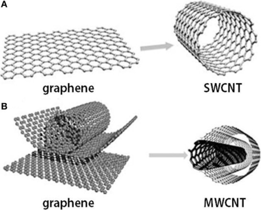
CNT is a tubular shaped material, made of carbon, having diameters measurable on the nanometer scale. They have a long and hollow structure and are formed from sheets of carbon that are one atom thick. It is called “Graphene”. Carbon nanotubes have varied structures, differing in length, thickness, helicity, and the number of layers. Majorly, they are classified as Single Walled Carbon Nanotube (SWCNT) and Multi-Walled Carbon Nanotube (MWCNT). As shown in Figure 3(a), one can see that SWCNTs are made up of a single layer of graphene, whereas MWCNTs are made up of multiple layers of graphene.


Properties of Carbon Nanotube
The carbon nanotube delivers excellent properties in areas of thermal and physical stability as discussed below:
1. Both Metallic and Semiconductor Behavior
The CNT can exhibit metallic and semiconductor behavior. This change in behavior depends on the direction in which the graphene sheet is rolled. It is termed as chirality vector. This vector is denoted by a pair of integer (n, m) as shown in Figure 3(b). The CNT behaves as metallic if ‘n’ equals to ‘m’ or the difference of ‘n’ and ‘m’ is the integral multiple of three or else it behaves as a semiconductor .
2. Incredible Mobility
SWCNTs have a great potential for application in electronics because of their capacity to behave as either metal or as a semiconductor, symmetric conduction and their capacity to carry large currents. Electrons and holes have a high current density along the length of a CNT due to the low scattering rates along the CNT axis. CNTs can carry current around 10 A/nm2, while standard metal wires have a current carrying capacity that is only around 10 nA/nm2.
3. Excellent Heat Dissipation
Thermal management is an important parameter for the electronic devices’ performance. Carbon nanotubes (CNTs) are well-known nanomaterials for excellent heat dissipation. Moreover, they have a lesser effect of the rise in temperature on the I-V characteristics as compared to silicon.
CNT in Transistor Applications: CNFET
The bandgap of carbon nanotubes can be changed by its chirality and diameter and thus, the carbon nanotube can be made to behave like a semiconductor. Semiconducting CNTs can be a favorable candidate for nanoscale transistor devices for channel material as it offers numerous advantages over traditional silicon-MOSFETs. Carbon nanotubes conduct heat similar to the diamond or sapphire. Also, they switch more reliably and use much less power than silicon-based devices.
In addition, the CNFETS have four times higher trans-conductance than its counterpart. CNT can be integrated with a High-K material, which is offering good gate control over the channel. The carrier velocity of CNFET is twice as compared to MOSFET, due to increased mobility. A carrier mobility of N-type and P-type CNFET is similar in offering advantages in terms of same transistor size. In CMOS, PMOS (P-type metal-oxide-semiconductor) transistor size is approximately 2.5 times more than NMOS (N-type metal-oxide-semiconductor) transistor as mobility values are different.
The Fabrication process of CNTFET is a very challenging task as it requires precision and accuracy in the methodologies.Here we discuss the Top-gated CNTFET fabrication methodology.
The first step in this technique starts from the placement of carbon nanotubes onto the silicon oxide substrate. Then the individual tubes are isolated. Source and drain contacts are defined and patterned using advanced lithography. The contact resistance is then reduced by refining the connection between the contacts and CNT. The deposition of a thin top-gate dielectric is performed on the nanotube via evaporation technique. Lastly, to complete the process, the gate contact is deposited on the gate dielectric.

Challenges of CNTFET
There are lots of challenges in the roadmap of commercial CNFET technology. Majority of them have been resolved to a certain level, but a few of them are yet to be overcome. Here we will discuss some of the major challenges of CNTFET.
1. Contact Resistance
For any advanced transistor technology, the increase in contact resistance due to the low size of transistors becomes a major performance problem. The performance of the transistor degrades as the resistance of contacts increases significantly due to the scaling down of transistors. Until now, decreasing the size of the contacts on a device caused a huge drop in execution — a challenge facing both silicon and carbon nanotube transistor technologies.
2. Synthesis of Nanotube
Another challenge with CNT is to change its chirality such that it behaves like a semiconductor. The synthesized tubes have a mixture of both metals and semiconductors. But, since only the semiconducting ones are useful for qualifying to be a transistor, engineering methodologies need to be invented to get a significantly better result at separating metal tubes from semiconducting tubes.
3. To develop a non-lithographic process to place billions of these nanotubes onto the specific location of the chip poses a challenging task.
Currently, many engineering teams are carrying out research about CNTFET devices and their logic applications, both in the industries and in the universities. In the year 2015, researchers from one of the leading semiconductor companies succeeded in combining metal contacts with nanotubes using “close-bonded contact scheme”. They achieved this by putting a metal contact at the ends of the tube and making them react with the carbon to form different compounds. This technique helped them to shrink contacts below 10 nanometers without compromising the performance.
Gate-All-Around FET: GAAFET
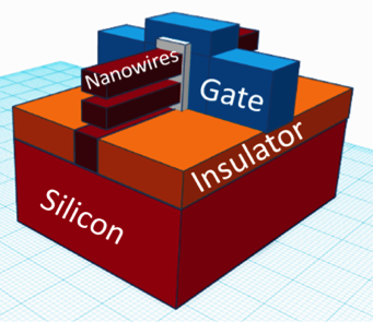
One of the futuristic potential transistor structures is Gate-all-around FET. The Gate-all-around FETs are extended versions of FinFET. In GAAFET, the gate material surrounds the channel region from the four directions. In a simple structure, a silicon nanowire as a channel is wrapped by the gate structure. A vertically stacked multiple horizontal nanowires structure is proven excellent for boosting current per given area. This concept of multiple vertically stacked gate-all-around silicon nanowire is shown in Figure 5.

Apart from silicon material, some other materials like InGaAs, germanium nanowires can also be utilized for better mobility.
There are many hurdles for GAAFET in terms of complex gate manufacturing, nanowires, and contacts. One of the challenging processes is fabricating nanowires from the silicon layer as it requires a new approach for the etching process.
There are many research labs and institute working for Gate-all-around FET for lower nodes. Recently, Leuven based R&D firm claimed that they achieved excellent electrostatic control over a channel with GAAFET at sub 10nm diameter nanowire. Last year, one of the leading semiconductor companies unveiled a 5nm chip, which contains 30 billion transistors on a 50mm2chip using stacked nanowire GAAFET technology. It claimed to achieve 40% improvement in performance compared to 10nm node or 70% improvement in power consumption at the same performance.
Compound Semiconductors
Another promising way to scale down a transistor node is the selection of novel material that exhibits higher carrier mobility. A compound semiconductor with ingredients from columns III and V are having higher mobility compared to silicon. Some compound semiconductor examples are Indium Gallium Arsenide (InGaAs), Gallium Arsenide (GaAs), and Indium Arsenide (InAs). According to various studies, integration of compound semiconductor with FinFET and GAAFET showing excellent performance at lower nodes.
The main concerns with compound semiconductor are large lattice mismatch between silicon and III-V semiconductor, resulting in defects of the transistor channel. One of the firms developed a FinFET containing V-shaped trenches into the silicon substrate. These trenches filled with indium gallium arsenide and forming the fin of the transistor. The bottom of the trench is filled with indium phosphide to reduce the leakage current. With this trench structure, it has been observed that defects terminate at the trench walls, enabling lower defects in the channel.
Conclusion
From the 22nm node to 7nm node, FinFETs have been proven successful and it may be scaled down to one more node. Beyond that, there are various challenges like self-heating, mobility degradation, threshold flattening, etc. We have discussed how carbon nanotube’s excellent properties of motilities, heat dissipation, high current carrying capability offer promising solutions for replacing existing silicon technology. As the stack of horizontal nanowire opened a “fourth gate”, Gate-all-around transistor structure is also a good candidate for replacing vertical Fin structure of FinFET for achieving good electrostatic property. It is not clear what comes next in the technology roadmap. However, in the futuristic transistor technology, there must be changes of existing material, structure, EUV (Extreme ultraviolet) lithography process, and packaging to sustain Moore’s law.
Accelerate early chip design and verification at lower technology node for faster time-to-market


