The global market of 3D ICs was valued at US$ 7,521.4 Mn in 2019 and is forecasted to reach a value of US$ 38,252.9 Mn by 2027 at a CAGR of 22.5% between 2020 and 2027.

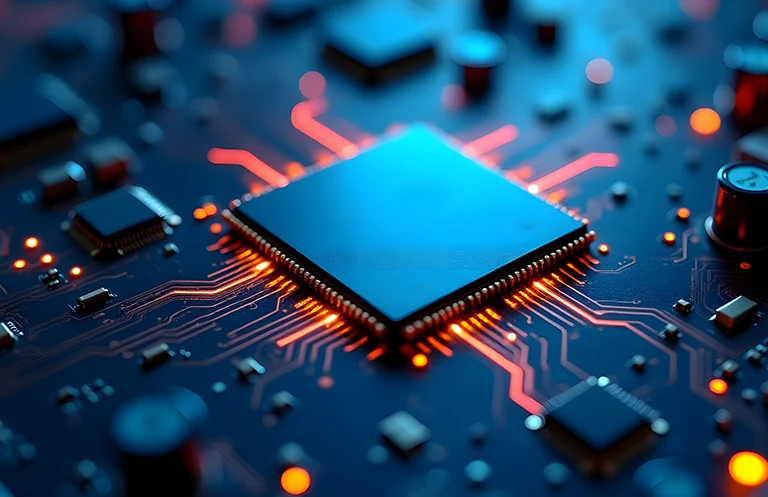
The basic definition for 3D ICs is logic over the logic that is connected through TSV. This includes a 3D memory i.e. a memory in the hybrid chip, which has the combined elements of 2.5D with 3D ICs. 3D IC technology can simulate a passive layout structure such as transmission lines and inductors. It also helps in creating high performing, low power consumption microchips.
In the networking industry, high-performance devices require a large storage capacity and bandwidth. In order to maintain these memory and bandwidth challenges, 3D ICs are considered as the ideal solution because, with 3D integration technology, the semiconductor industry gets the high bandwidth benefits and chip density offering. The adoption of 3D IC technology is dependent on the need for interconnecting density and cost factors.
With the increasing demand for 3D ICs, let’s discuss its role in various emerging technologies:
1. In Consumer Electronics
Several companies from the semiconductor design industry such as fabs and foundries are looking for heterogeneous integration of chip components (3D ICs) to polish the user experience and trying to grow with the popularity of the consumer electronic market
In the miniaturization of consumer electronic device market, semiconductor design companies are facing various challenges to enhance performance, low power consumption, while reducing chip size to 7nm, 5nm and below. In order to overcome these challenges in lower technology node design, semiconductor companies pursuing 2.5D and 3D ICs to consumer electronic products which provide 30% saving power consumption, a 40% increase in performance and cost reduction by 5-10%. For consumer electronics, through TSV technology, 3D ICs helps in:
- Enhancing memory capability and bandwidth
- Low power design
- Dynamic thermal management (DTM)
- High speed data management of denser chip
- Enabling connected and smart devices
In the region of 3D ICs, a 3D imaging ASIC is designed specifically for use in 3D vision applications, which includes those parameters that are used for consumer devices like smartphones, tablets, laptops, and personal computers.
In 3D imaging, it includes two lenses which are used simultaneously for capturing 3D shape data at every short. This shows that 3D images having a huge amount of data with grater image depth as compared to 2D images. Several IC sector products are expected to adopt 3D IC technology like MEMS & sensors, RF SiP, Logic (3D SiP / SoC), and much more.
In chip design flow, 2.5D and 3D ICs with TSVs provide enhanced electrical performance due to the very high number of TSV interconnections and short interconnects within stacked circuits. This drives a wave of growth in the global 3D ICs technology sector.
The above mentioned factors are expected to propel the consumer electronic market growth shortly.
2. In Machine Learning (ML)
From voice assistant speakers (Amazon’s Alexa, Google Home, Siri, etc.) to self-driving cars, Artificial Intelligence/Machine Learning (AI/ML) is rapidly influencing our daily lives.
As lower technology node design goes down from 16nm to 7nm, 5nm, and 3nm in the future, variation becomes a major challenge that has to be addressed for all types of design techniques including 3D ICs. The key to using the machine learning technique in 3D ICs is to develop a fast and accurate simulation variation model for 3D ICs by replacing with 2D ICs computationally expensive simulation.
Machine learning has recently been applied to 3D stacked IC design in various means:
- Improving chip optimization by using efficient configurations of software tools
- Predicting the areas on a chip that can experience manufacturing defects
- Scaling down the voltage in order to save power by predicting the load on a CPU
- Had an impact on the EDA tools also which helps in a lower cost of designs and faster time to market by allowing tools to suggest solutions to common problems in the chip design flow.
EDA companies like Cadence and Synopsys are working on routing and tuning of 3D ICs in order to improve reliability, power, performance, and area (PPA) results by using machine learning analytics, and optimization techniques.
3. In Artificial Intelligence (AI)
In the miniaturization period, many AI experts believe that the next evolution will deliver smart technology to understand smart designs in smart surveillance, smart homes, smart wearable, and smart wireless devices for integrated smart devices.
With the rise of AI, the semiconductor industry has been energized across multiple applications in diverse markets. Likewise, the SEMI industry association is forecasting that AI and 5G cellular communication will be the major growth drivers pushing the semiconductor market to over $500 Bn by the end of the current year.
In the semiconductor industry, AI is considered a key enabler in smart functionality and advances the semiconductor methodologies for sensors and lower technology node design capabilities.
Due to the demand for lower technology node design i.e. more capable and increasing demand of AI powered IoT devices, semiconductor industry moving to 3D-IC integration or 2.5D-IC integration which are optimized with system-in-package (SiP) and multi-functional devices, where die placed side-by-side or stacked which helps in handling AI applications.
In this huge industry, along with Moore’s law, future AI will be a new growth driver with their new optimization techniques, new hardware/software platforms and could be built into increasingly smaller devices.
Conclusion
In this blog, the author explains about the 3D IC growth in emerging technologies like consumer electronics and AI/ML. This will drive market growth, and enhance power, performance, and area by using ML/AL optimization techniques and algorithms in the era of miniaturization (16nm, 14nm, 7nm, 5nm and below).
eInfochips has over two decades of experience in providing product engineering and ASIC/FPGA design services. The team also moving from 2D to 2.5D and 3D IC technology for different markets like AI-driven datacenters, Networking systems, Consumer electronics, storage applications, and much more.
Looking for 2.5D and 3D IC technology integration capabilities?