


AI-driven chip design means applying artificial intelligence and machine-learning methods across semiconductor design workflows to help with bounded optimization, search, classification, and engineering assistance in tasks such as RTL drafting, floorplanning, verification, routing, analog design, and post-silicon test. AI is making its way into virtually every corner of chip design, but the evidence supporting its effectiveness and its level of maturity varies considerably depending on the task. The most practical and well-established applications currently are bounded optimization, search, classification, and engineering assistance, among others. Generative and agentic workflows, on the other hand, are new to the scene and need careful, hands-on validation before teams can rely on them with confidence.
For semiconductor design engineers, verification teams, chip development professionals, and readers tracking how AI fits into EDA, the useful question is not whether AI can “design a chip” end to end, but where it measurably improves productivity and decision-making inside a validated flow. Describing Artificial Intelligence (AI) in semiconductor design as a straight shot from specification to finished chip is an appealing idea, but the reality is a lot more grounded. Most of the tools we hear about in practice are built to work within a specific stage or workflow, where goals can be clearly measured, and outputs can be validated using established EDA methods.
That distinction is worth paying attention to because modern chip programs involve large design spaces, repetitive verification loops, and hard timing, power, and physical tradeoffs that benefit from faster search and better ranking not less rigor. A model can scan thousands of implementation options, rank regressions, or cluster failures without ever being handed over final authority of design. Whatever it produces lives inside a broader engineering process, one that includes simulation, formal verification, sign-off checks, and human review every step of the way.
This article follows those AI applications across the chip design lifecycle, from RTL and testbench generation to floorplanning, physical implementation, routing, timing and power closure, analog optimization, sign-off, tape-out review, post-silicon validation, and emerging cross-lifecycle agents and engineering copilots.
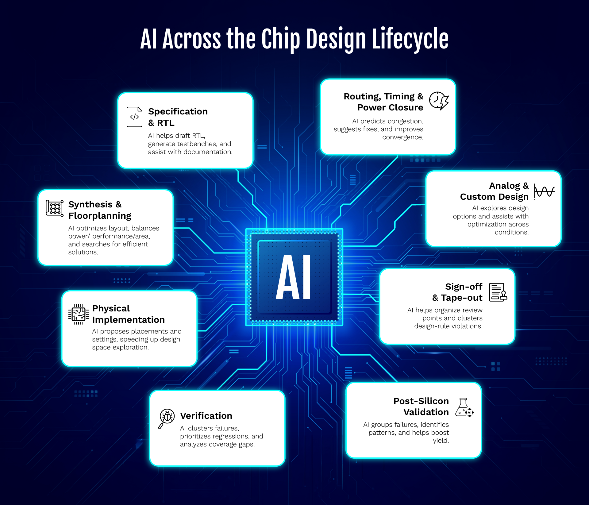
1.Specification, architecture, and RTL in chip design: useful assistance, not hands-off design
Generative AI is entering front-end design through documentation assistance, script generation, RTL drafting, refactoring, assertions, and testbench support. Synopsys lists RTL and formal-testbench generation among the capabilities of Synopsys.ai Copilot.[1] Cadence describes ChipStack AI workflows for generating or refactoring RTL and testbenches from specifications and existing design content.[2] These are vendor-stated capabilities; the usable scope and level of automation depends on the design, data, tool setup, and review process.
The potential value is straightforward. Engineers spend substantial time turning requirements into executable design intent, writing repetitive code, and setting up verification infrastructure. A domain-aware model may help create a first draft, explain unfamiliar code, or provide a starting point for a testbench.
The limitation is correctness. Hardware code is not judged by whether it looks plausible. It must be functionally correct, synthesizable, efficient, and aligned with timing, power, reset, clocking, and safety requirements. Public benchmarks continue to show a substantial gap between successful examples and dependable automation on complex tasks. The 2025 Comprehensive Verilog Design Problems benchmark reported that leading models achieved no more than 34% pass@1 on its code-generation tasks, with agentic reuse and verification tasks proving especially difficult.[3] A larger benchmark published in June 2026 reinforced these findings, reporting similarly low success rates on more complex RTL reasoning and issue-fixing tasks.[4]For the time being, the practical takeaway is this: GenAI can meaningfully support selected block-level tasks, but any generated content demands the same rigorous treatment as human-written RTL. That means linting, simulation, formal checks, synthesis, thorough review, and clear traceability back to the original specification.
2.Synthesis, floorplanning, and placement: a more established optimization use case
Physical implementation is a natural area for machine learning to contribute, largely because it involves an enormous search space with objectives that can be measured. Power, performance, and area all need to be balanced against constraints that interact in ways that are not always intuitive. Human experts are essential, but manually testing every combination of floorplan, placement, synthesis settings, and tool configurations is not practical.
Google’s published research on floorplanning illustrated the core idea: reinforcement learning can draw on prior designs to quickly propose layouts that hold up well against defined metrics.[5] Commercial vendors have described related approaches for exploring the design space. Synopsys states that DSO.ai uses reinforcement learning to explore PPA outcomes, and Cadence describes Cerebrus as a system for evaluating implementation options relative to design goals.[6, 7]
Compared to generative RTL work, this category has a longer public track record and is more directly tied to measurable EDA outputs. The model proposes settings or searches for solutions, while implementation and sign-off tools calculate the actual results. Engineers continue to define constraints, evaluate feasibility, review trade-offs, and make the final call. Real-world gains vary considerably depending on the specific design and how the flow is set up.
3.Verification: a practical area for artificial intelligence-assisted productivity
Verification produces large amounts of structured data, including regressions, coverage metrics, assertions, error logs, waveforms, and recurring failure patterns, and AI can analyze those signals to identify bugs earlier. The work is also iterative and resource-heavy, which makes it a reasonable area for AI-assisted prioritization and analysis.
Vendor documentation points to several current applications: regression prioritization, coverage analysis, failure clustering, triage, and root-cause assistance. Synopsys positions VSO.ai around coverage closure and regression efficiency.[8] Cadence describes Verisium as targeting workload optimization, coverage, failure triage, and debug.[9] The actual scope and results vary depending on the verification environment and how the tools are set up.
Portable Stimulus Standard (PSS) helps define comprehensive hardware-software interaction scenarios, including synchronization points for co-operability, and supports broader testing across those boundaries. Traditional verification methods often miss issues at the hardware-software boundary, and debugging mixed hardware-software environments is especially complex; PSS adoption is increasing as electronic systems become more complex.
These systems do not remove the need for verification planning or a solid understanding of the specification. What they do is reduce the amount of manual sorting that surrounds the engineering work. That is an important distinction. The value typically comes from helping a verification engineer get to the right failure or coverage gap more quickly, not from replacing the verification environment.
4.Routing, timing and, power: predicting trouble before the last mile
Backend design is notorious for late-stage feedback loops. Congestion can force routing changes, which in turn affect timing and power. Fixing one timing path can introduce another violation, and at advanced nodes, even small physical changes can ripple across many corners and modes.
AI and machine-learning methods are being applied to problems like congestion and design-rule prediction, as well as implementation-option ranking and trade-off exploration before teams commit to lengthy tool runs. These approaches can also draw data from previous runs to identify settings that performed well on similar blocks. In timing and power closure, the practical goal is better convergence and predictability rather than a fully automated answer.
The same logic holds for engineering change orders. A recommendation engine can narrow down the most likely fixes, but each change must be implemented, analyzed, and signed off. How useful that guidance turns out to be depends heavily on the design context and the quality of historical data the model has to work with.
5.Analog and custom design: optimization across many corners
Analog design introduces a similar combinatorial challenge, albeit in a different form. A circuit may need to satisfy many performance measurements across a wide range of processes, voltage, and temperature conditions. Synopsys describes ASO.ai as using reinforcement learning and optimization to explore the design space, including hierarchical designs and post-layout parasitics. Siemens, meanwhile, describes Solido as applying machine learning to specific analog and custom-IC workflows involving verification, characterization, and optimization.
None of these reduce the importance of analog expertise. What it does is allow experienced judgment to scale further. The engineer selects the topology, defines the measurements, understands how failures can occur, and determines whether a statistically strong solution is physically sound and robust enough for the product.
6.Sign-off and tape out: helping teams review large result sets
Final physical verification can generate an enormous number of violations and review points. Siemens describes Calibre Vision AI as a system that processes and clusters design-rule-check results so that related issues can be examined together.[13] When applied carefully, approaches like this can help teams organize their review workload and direct engineering attention where it matters most before the final tape out decision.
The sign-off criteria themselves remain non-negotiable. DRC, LVS, static timing, power integrity, and reliability checks continue to be rule-based and accountable. AI contributes to prioritization, pattern recognition, and debugging those checks. It does not change the definition of what constitutes a passing design.
7.Post-silicon validation, test, yield and reliability: valuable data, fragmented workflows
After a chip is fabricated, teams encounter different kinds of data challenges. They must work with lab measurements, tester output, failing units, firmware logs, environmental conditions, and manufacturing history. AI methods can help by grouping similar failures, identifying correlations, supporting investigations into potential design or process causes, and improving manufacturing yields by detecting defects and optimizing production-related processes to protect product quality. Synopsys describes TSO.ai as a test-space optimization application that looks for ways to reduce pattern count and test turnaround time.[14]
Yield and reliability analysis are harder to standardize because the relevant data is typically spread across separate organizations, including design teams, foundries, OSATs, test engineering groups, and product teams. Data volumes can be large, yet labels are often weak, and access is tightly controlled. These factors explain why post-silicon and yield intelligence remain far less standardized than physical-design optimization.
8.Cross-lifecycle intelligence and engineering copilots: an emerging layer
Most chip programmes organize knowledge by tool, stage, and project. A timing decision made during implementation may have no clear connection to a failure discovered in the lab. A verification workaround may never be turned into reusable guidance for the next design team. The long-term value of AI lies not only in automating individual tasks but in making those connections easier to surface and act on.
EDA vendors have continued to announce agentic and multi-agent capabilities. Synopsys presented an AgentEngineer-based multi-agent workflow in March 2026. Cadence announced further extensions to ChipStack AI in June 2026. Siemens launched the Fuse EDA AI Agent in March 2026. [15, 16, 17] These announcements show where vendors are directing their investment, but public evidence on broad production use, repeatability, and results across varied design environments remains limited.
Terms like “autonomous design” therefore deserve careful reading. Some vendor offerings are described as operating at high levels of autonomy within specific workflows, but chip development involves many interdependent requirements, approval points and sign-off obligations. In practice, engineers remain responsible for setting objectives and constraints, carrying out reviews and validation, and making final decisions.
A simple maturity view
| Design stage | Current public maturity | Typical publicly described use | What still needs close engineering control |
| RTL and testbench generation | Early / emerging | Drafting, refactoring, assertions, scripts, and documentation assistance | Functional correctness, architecture, design quality, and sign-off |
| Floorplanning and implementation optimization | Commercially available; results are project-dependent | Design-space exploration and PPA trade-off analysis | Constraints, feasibility, final selection, and sign-off |
| Verification and debug | Commercially available in selected workflows | Regression optimization, coverage analysis, triage, and debug assistance | Verification strategy, test intent, and bug disposition |
| Routing, timing, and power closure | Commercially available as assisted optimization | Prediction, option ranking and convergence support | Cross-corner judgment and closure accountability |
| Analog optimization | Commercially available for bounded search and analysis | Multi-objective exploration across defined PVT conditions | Topology, specifications, robustness, and physical judgement |
| Post-silicon, yield, and reliability | Developing; adoption is uneven | Failure clustering, correlation and test optimization | Data quality, causal analysis, and cross-company collaboration |
| Crossflow agents and copilots | Early / newly announced | Tool guidance, workflow orchestration, and knowledge retrieval | Governance, context, security, validation, and final decisions |
What “measurable impact” really means
There is no single percentage improvement that applies universally across chip programs. Outcomes depend on design size, node, methodology maturity, compute budget, starting quality, available data, and how well a given capability fits into the specific workflow. The most credible way to talk about impact is at the task level: fewer redundant simulations, faster failure triage, fewer implementation iterations, earlier visibility into risk, or better PPA on a defined block.
AI is starting to influence parts of the design flow, but its role is best understood as assisted intelligence working alongside established engineering tools. A simple test helps clarify where it can be used responsibly: the more clearly a task can be measured and independently verified, the more straightforward it becomes to apply AI within that task.
Next in the series: The Underpinning Semiconductor Ecosystem
Frequently Asked Questions – AI-Driven Chip Design Lifecycle
1. Where is AI currently used in the chip design lifecycle?
AI is now present across multiple stages of chip development, from RTL assistance and physical design optimization to verification, timing and power closure, analog design, sign-off analysis, and post-silicon testing. Its most established contributions lie in search, optimization, prediction, and failure analysis rather than in fully autonomous chip design.
2. How is AI used in semiconductor verification?
AI supports verification teams by helping them prioritize regressions, identify coverage gaps, cluster related failures, analyze logs, and investigate root causes. These capabilities can cut down on manual triage and allow engineers to focus their attention where it matters most. That said, verification strategy, test intent, and final bug disposition remain firmly in the hands of engineers.
3. Can AI generate production-ready RTL and testbenches?
AI can assist with drafting RTL, refactoring code, writing assertions, creating scripts, and building testbenches, but none of this output is automatically ready for production. Generated content needs to go through linting, simulation, formal verification, synthesis, design reviews, and traceability checks against the original specification before it can be trusted.
4. Which AI applications are most mature in semiconductor design?
Some of the more commercially established applications include AI-assisted floorplanning, implementation optimization, verification analytics, test optimization, and result classification. Generative RTL, crossflow copilots, and agentic design workflows are in earlier stages of development and calls for tighter controls, well-secured engineering data, and careful human oversight throughout the process.
Sources and further reading
1. Generative AI for Chip Design — Synopsys. RTL and formal-testbench generation capabilities.
2. AI for Design — ChipStack AI Super Agent — Cadence. Agentic RTL, testbench and debug workflows.
3. Comprehensive Verilog Design Problems — NVIDIA Research / arXiv. Benchmark of LLM and agent performance on hardware design and verification.
4. RTL-BenchLS: A Large-Scale Benchmark for RTL Reasoning and Generation — arXiv. June 2026 benchmark covering more complex RTL tasks.
5. A graph placement methodology for fast chip design — Nature. Reinforcement-learning floorplanning research.
6. DSO.ai — Synopsys. AI-driven design-space optimization.
7. Cadence Cerebrus Intelligent Chip Explorer — Cadence. Automated PPA-oriented design-flow optimization.
8. VSO.ai — Synopsys. Coverage closure and regression optimization.
9. Verisium AI-Driven Verification Platform — Cadence. Verification workload, coverage and debug applications.
10. How NVIDIA Uses Functional Verification Tools — Synopsys. Vendor-reported NVIDIA coverage-closure case study.
11. ASO.ai — Synopsys. AI-assisted analogue design optimization.
12. Solido Design Environment — Siemens. AI-powered custom-IC verification and optimization.
13. Calibre Vision AI — Siemens. AI-assisted DRC analysis and clustering.
14. TSO.ai — Synopsys. Semiconductor test-space optimization.
15. Synopsys Outlines Vision for Engineering the Future — March 2026 company announcement describing an AgentEngineer-based multi-agent workflow for design and verification.
16. Cadence Unveils Fully Autonomous Virtual Engineer for Chip Design — June 2026 company announcement describing an extension of the ChipStack AI framework; capability and performance statements are vendor-reported.
17. Siemens launches Fuse EDA AI Agent — March 2026 company announcement describing multi-tool workflow orchestration for semiconductor and PCB design.