1. Introduction
Effect of charge accumulation in isolated nodes of an integrated circuit during its processing is known as Antenna effect. This effect is also known as Plasma Induced Damage. The discharging of accumulated charges, which is done through the thin gate oxide of the transistor, it might cause damage to the chip and degrade its performance. During the fabrication process, we need to etch out the unwanted oxide layer from the wafer, which can be done using plasma etching. Plasma contains high energetic ions and radicals for etching that get collected by interconnect. The amount of charge accumulation depends on the surface area of interconnects. These collected ions increase the potential of interconnects and if the interconnect is connected to gate, a drainage path could be formed through the gate oxide to balance out the charge collection depending upon the amount of charge collected by interconnects. The drainage path could either breakdown the gate oxide, which may lead to permanent damage of the device. During the plasma etching of interconnect, positive ions and neutral species from the plasma get strikes at interconnector these are collected by the interconnects, so if the area of the interconnect connected to the gates is large enough then the potential of the interconnect or poly silicon maybe large enough that it could breakdown the gate oxide.
2. Etching
Etching refers to the removal of material from the wafer surface. There are two main types of etching:
- Wet etching: Wafers are immersed in an etchant solution (mixture of chemicals). A chemical reaction occurs between the wafer surface and the etchants that helps in material removal.
- Dry etching: In this, plasma or etchant gasses remove unwanted material. This reaction that take place which can be done by utilizing high kinetic energy of particle beam or chemical reaction.
3. Plasma Etching
In this process, chemical etchant is introduced in the gas phase. For etching silicon oxide, CF4 (tetrafluoromethane) is used. In a chamber, there are two electrodes; one is holding a wafer and a very high electric field created between these two electrodes. The chamber is first evacuated before introducing the gas. Radio frequency electrodes are then used to generate the plasma that ionizes the gas. This ionized gas attacks the oxide layer and remove the layer.
When high energetic ions beam are bombarded on the target that dislodge portion of the material from the exposed surface.
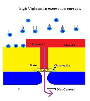
4. Flow of finding antenna violations: Inputs and Outputs.

- Antenna rules: Foundry provides the antenna rule file, which must be followed during the chip layout design. In the antenna rules most common rule is Antenna Ratio same as shown in fig2. Antenna ratio is the ratio of metal area connected to the gate to the total area of gate.Antenna area/gate area < Maximum Antenna Ratio
- Antenna Violations: Long metal lines and Vias introduce antenna violations. The antenna rule specifies the maximum tolerance for the ratio of a metal line area to the area of connected gates. VLSI process starts from the substrate, device layer and then metal layers. The Etch process builds up the electrical charges on metal layers. These charges cause a high voltage spike, which may damage the gates connected to the metals. Gate area is the multiplication of channel length and channel width. Antenna problem is due to Bottom area and parameter of the metal line. Via and contact also contributes to the antenna violations. There are three kinds of antenna violations in the system-on-chip design:
- Metal area antenna rule: The maximum limit to the ratio of the metal line area to the connected gates area.
- Perimeter antenna rule: The maximum limit to the ratio of the metal line perimeter connected gates area.
- Via or contact area: The maximum limit to the ratio of the via or contact area to the connected gates area.
Violations to the above antenna rules in every metal layer have to be fixed before the chip tape out. Fig 3 shows the design layout of one piece of metal connected to a poly gate. The poly gate with L and W for gate length and gate width and gate area is W*L. The perimeter antenna ratio for figure is defined as follows:
R=(P*T)/(W*L)
In fig 3, P is the sum of the periphery length for the metal as shown in figure. T is the thickness of the metal. W and L are the gate width and gate length. The perimeter antenna rule specifies the upper limit for R. If we increase the W or L for gate or decrease P for metal line, the ratio R is reduced. Each metal layer may have various upper limit to R based on the process specifications.

5. Antenna Preventions
Techniques to fix the antenna violations as follows:
- Routing on Higher Metal Layer: Long metal can be taken to higher metal routing layer. This is known as metal jumping. This metal jumping is usually done near to the load. This metal jumping will break the long interconnect and hence the charge collected on the long interconnect will not discharge through gate oxide because the higher metal layer is not yet fabricated. This solution may increase the routing congestion on higher metal layer (see fig4.)
- Reduce the via-area: Large via area also results in process antenna violation. Converting multi-cut vias to double-cut via or double-cut vias to single-cut via reducing the cut area. This may impose serious reliability issues such as electromigration.
- Diode Insertion: Diode helps dissipate charges accumulated on metal. Diode should be placed as near as possible to the gate of device on low level of metal. Connecting a diode to the gate electrode which provides a discharging path for the static charge present on the metal layer. Diode should always be connected in reverse bias, with cathode connected to gate electrode and anode connected to ground potential.
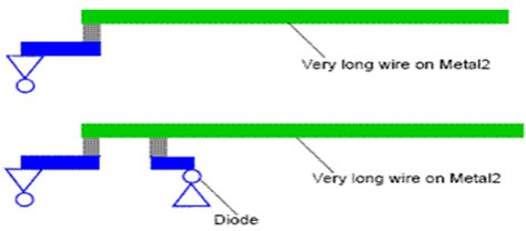
6. Application:
Chip is on 16 nm technology which is being operated at 1GHZ and its size is 7900.0 x 3244.0
We faced Some Antenna violations while working on it.
- Via Area: Violation due to via area which was routed on higher metal let’s say on M8 and M9 and its net respectively. It was sorted by changing the routing from higher metal routing layer M8 and M9 to lower Metal routing layer let’s say M6 and M7. As shown in fig5 and fig6 via area is reduced.
- Metal Area: Violation due to long Metal routing layer let’s say it is on M8, which was resolved by breaking this layer and connected by inserting jumper near to the load. It can also be resolved by inserting diode (Reversed Biased) near to the load.
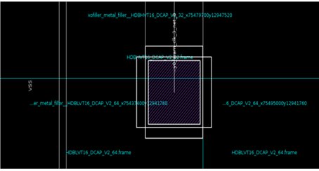
via89_1cut
via area: 0.219
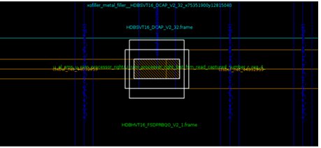
Via67_Long_H
via area: 0.0168
7. Conclusion:
In this blog, author discussed about the antenna effect due to plasma etching and different PV tools used to identify antenna effect by comparing design GDS and antenna rule file provided by foundry. And by adding diode, routing to upper metal layer and reducing via area, can solve the antenna violation.
Tool Used: IC Validator, ICC2
REFERENCE
[1] Peter H. Chen and Sunil Malkani, Chun-MouPeng, James Lin, Fixing Antenna Problem by Dynamic Diode Dropping and Jumper Insertion.
[2] Jean-Pierre Carrère, Jean-Claude Oberlin, Sylvie Bruyère, Paul Ferreira plasma damage in ultra-thin gate oxide induced by dielectric deposition processes: An overview on main mechanisms and characterization technique.
Upma Pawan Kumar & Sunandan Choubey


