Globally, engineering teams have been working cooperatively toward making futuristic advanced technologies in minute-sized ASIC (Application Specific Integrated Circuit). This exciting race is full of challenges of finding compact, faster, and more efficient Integrated Circuit (IC) designs to construct future technologies. In a report published in Grand View Research, the size of the worldwide Application-Specific Integrated Circuit (ASIC) market was assessed at USD 15.99 billion in 2022, and from 2023 to 2030, it is anticipated to expand at a CAGR of 5.9%.
Application-Specific Integrated Circuit (ASIC): What are they?
ASIC design is a process of reducing the size and cost of an electronic circuit, a product, or a system. It happens by reducing and integrating a single component and its performance into an individual element.
An electronic product often combines many ICs (Integrated Circuits) and they are conjoined to perform a specific function. For example, in the 1980s smoke detectors were made of common-purpose ICs, such as comparators, amplifiers, and regulators. It was huge and had a lot of components and assembly costs. With boosted competition, the necessity for cost-efficiency and small size steers the need for merger and integration of all individual components into a single ASIC, which not only reduces the size and cost of the smoke detector but enhances its dependability.
As per Moore’s law, the count of transistors and gates doubles every 18 months, and it is increasing in high density per integrated circuit. The following 15 years will see more advancement in technology as parallelization, CAD tools, logic, and memory all accelerate.
eInfochips has worked with a client who was planning to design a second-generation chip, with programmability above 10 Tbps based on a 7nm technology node. The client was looking for an engineering partner with this area of expertise. You can read more about this case.
ASIC chip designs are of three types-
- Full Custom Design
- Semi-Custom Design
- Programmable ASIC
Prediction of VLSI evolution by Semiconductor Industries Association-
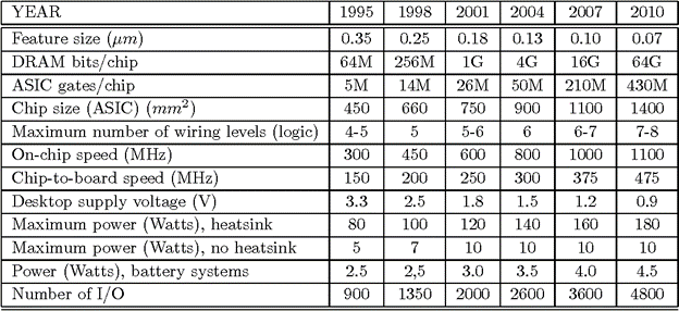
Image Source: Semantic Scholar
ASIC Design Process
ASIC Requirement
Customers of a semiconductor company use the chip in their final product and systems. Customers’ requirement is supreme while designing a chip. The first step would be to gather the requirements, figure out the value of the end product and assess the number of resources required for the project.
ASIC Specification
ASIC specification is a document that enliststhe product specifications before embarking on a journey of product designing. It also enumerates how a device should perform its functions in various operational situations. For example, the tithe specification phase is an important part of the designing and developing process. Now that technology is ingrained in every aspect of life, customers expect new design features, continuous improvements, high-speed processing, and low power consumption.
An expert in ASIC system design helps the customer in building the system architecture and specification. This process takes around two to six weeks depending on the difficulty type of the application requirement. The specification process has the following steps-
- Assessing the specification, system schematics, and block diagram
- Growing a better understanding of any design problem, challenges
- Concluding a decision related to the final product, not just ASICs
- Deciding on if any certification is needed in products such as IEC and TS compliance
- Creating the ASIC block diagram with its function components, specification
- Silicon integration by determining board-level architectural trade-offs
ASIC Architecture
Once all the specifications are clear, it is time to categorize the ASIC performance into multiple performance blocks. An architect’s work is to derive the best performance of the ASIC chip and minimize the hardware resources that directly help in maintaining the overall chip cost within the assigned budget. In this course, the architects define the relationship between different performance blocks and assign the time budget to each block.
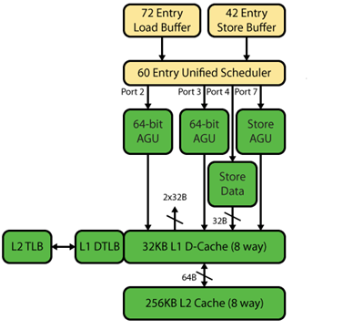
Image Courtesy: Real World Technology
Once it is clear what performance blocks are required, it is much easier to recognize the critical modules and ideation on whether you require to re-use those IPs from the previous projects or make any required changes to the existing IPs.
What Is Logic Design And Verification?
This is the foremost part of the ASIC design flow and it includes coding the data flow of all performance blocks in a hardware description such as Verilog, VHDL, or system Verilog. The logic design includes:
Combinational Logic: Combinational logic refers to Boolean combinatorial such as OR, AND, NAND, NOR, and so on. These gates are easy; hence they can also be united to carry out difficult digital operations.
Sequential Elements: Sequential elements play a crucial role in combining various combinational logic clouds executing different functions by keeping their output temporary. Sequential elements such as flip-flops and latches are referred to as memory elements and managed by a coincide circuit or a control signal referred to as a clock.
Finite State Machines (FSMs): These are an elevated abstraction of sequential logic that can be applied to both hardware and software. FSMs model retaliation of a digital machine to the set of inputs gives a deterministic set of outputs and is a crucial building block for the logic designers.
Arithmetic Logic Blocks: Arithmetic computations are usually an obstruction for performance in high-performance CPU cores. It comprises multiplication, subtraction, addition, and division. There are various ways to execute these circuits which provide an exchange between performance, area, and power. Whatever is convenient for their application and best suited, it can be selected by the logic designers and optimized for one or more parameters.
Data-Path Design: Hardware Description Language (HDL) can abstractly copy data path design like a programming language that can be translated by EDA tools correctly.
Analog Design: ASIC may have a lot of analog components that assist in interfacing with the real world and may include Temperature Sensors, Analog to Digital (ADC), and Digital to Analog Converters (DAC).
With the logic design, the verification team also needs to build a verification plan for both the digital and analog logic components. The team generates practical tests to check the design for all possible corner cases and ensure proper and consistent functionality with the application. Writing the Register-Transfer Level (RTL) coding takes 10-20% of the entire design cycle time, whereas verification accounts take 80-90% of the time.
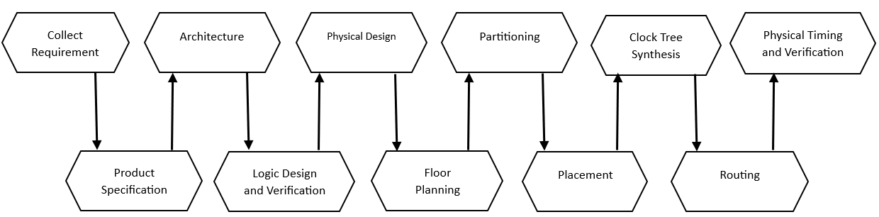
What Is Physical Design?
Physical design is also known as back-end design. It is the process of changing the gate-level netlist produced at synthesis into practical ASIC hardware. Physical design flow is sub-divided into the following-
Floorplanning: Floorplanning is the procedure to put the functional blocks in the chip area to assign a routing area between them, arrange for critical power and ground connection, and decide on Input/Output pad locations. A quality floorplan stabilizes design restrictions to decrease the total die area and improve signal routing channels to soothe layout and signal performance, and relative placement of the functional blocks to decrease interference and maintain signal integrity.
Partitioning: Partitioning is the procedure of splitting the chip into small blocks. The main agenda of partitioning is to construct the functional block easier for routing and placement.
Placement: Placement is the procedure of parting the chip into the smaller blocks by positioning them correctly with the standard cells by making sure nothing overlaps on the chip. There are four phases to perform the placement: pre-placement, in-placement, and post-placement before and after clock tree synthesis.
Clock Tree Synthesis
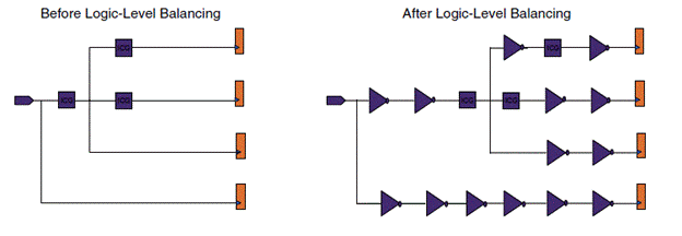
Image Courtesy: System to ASIC
Clock tree synthesis is an operation that confirms even allocation of clock signals to all the sequential elements in a design to avert clock timing-related errors. Clocking of gates in fast-moving designs are subject errors that occur because of the clock edge not appearing at the exact time it is expected to, compared to when it appears at other parts of the circuit. This timing error is called clock skew and it relies on several variables, both in the original design and physical execution.
Routing: Routing is an operation of attaching macros, I/O ports, power, standard cells, and the clock physically with metal traces. It is segregated into two steps: global and detailed routing.
Physical And Timing Verification
Logic verification ensures accurate performance and physical verification certifies accurate layout. There has been a rise in physical verification checks which comprise Design Rule Checks (DRS), Layout Versus Schematic (LVS), Shorts, and Floating nets. It is vital to track these breaches side by side with the place and route flow to steer clear of any hiccups just days before the tape-out.
Final Thoughts
If you perform the ASIC design process carefully, it is practicable to derive huge benefits in terms of decreasing the unit cost and enhancing the performance. However, if errors occur, the development cost increases, and further reiteration of the ASIC design and development process is required. Thus, you need utmost care to guarantee that ASIC development is accomplished. eInfochips has more than 25 years of experience in helping its clients in digital and mixed-signal ASIC design, and FPGA-SoCs development for different industries. We offer DFT/DFM services, architecture definition, and implementation, FPGA to ASIC conversion, pre-silicon validation, and post-silicon validation. To know about our key offerings and services read here and to contact our team of experts click here.