The use of mixed-signal processing is becoming vital among a wide variety of applications like telecommunication, networking, sensor chips, etc. In many designs, we have seen phase-shifted clocks being used by RTL designers. In a case where two flops are driven by phase-shifted clocks, we may not need to fix hold violations between them. When these flops are stitched together in a scan-chain using a single scan_clk, we will have hold violation during stuck-at capture. This leads to X-propagation through the compressor logic, causing coverage-loss. This article describes the challenges faced during DFT implementation for the above scenario.
Phase-Shifted Clocks
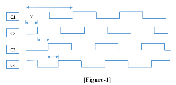
As a part of mixed-signal processing, many of the design uses phase-shifters circuits, which changes the phase-shift of the inputs by x degree. Below is one example of the phase-shifted clocks.

In the aspect of VLSI, consider a design where the flops have phase-shifted clocks and the frequency of the clock is same. As a nature of phase-shifted clocks, there will always be a delay between two positive/negative edges between two phase-shifted clocks as shown in Figure-1. It is important to understand the benefits as well as the challenges to be faced when the SoC is being designed using phase-shifted clocks.
The Static Timing Analysis (STA) checks the timing between critical paths in design and reports the violating paths which do not meet setup/hold criteria. Here, STA analysis can be seen in different ways when phase-shifted clocks are being used in the design. That is because sometimes the hold-violations cannot be seen due to sufficient delay between two edges of the phase-shifted clocks. This should be considered as an advantage of the phase-shifted clocks as it helps avoid unnecessary insertion of buffers/inverters in design.
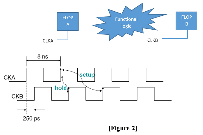
In the below figure, CLKA and CLKB are of the same frequency, but have different phases. Figure-2 shows how both the clocks are phase-shifted with the phase difference of 250ps.

In the VLSI field, mostly all SoCs use standard DFT insertion flows. When DFT is inserted for the design having phase-shifted clocks, there will be more challenges as compared to the standard DFT insertion flow.
DFT Challenges
Now, let us talk about DFT challenges for the phase-shifted clock design. In the scan mode, all the flops are converted into scan-flops and stitched together with a single ‘scan_clk’. During the transition-delay-ATPG (Automatic Test Pattern Generator), the functional clocks will toggle when SE (scan_enable) is low to produce launch and capture pulses. During Stuck-at ATPG capture, a single ‘scan_clk’ is triggered in the functional mode as shown in Figure-3.

Since the phase-shifted clocks are pulsed in functional mode, there is no need to fix hold violations. However, this will cause problems in scan-mode when the single ‘scan_clk’ will be pulsed for all scan-flops when SE is low. Due to this, both scan-flops FlopA and FlopB shown in Figure-2 will capture data at the same time, causing hold-violations.
One may opt to put delay-cells to resolve hold violations in SCAN mode, but it may require a huge number of delay-cells. In such cases, single capture pulse of ‘scan_clk’ will cause hold violations and capture X on scan-flops. It will further propagate into scan-chains and XOR-compressor logic, resulting in coverage-loss.
Approach to Fix DFT Challenges
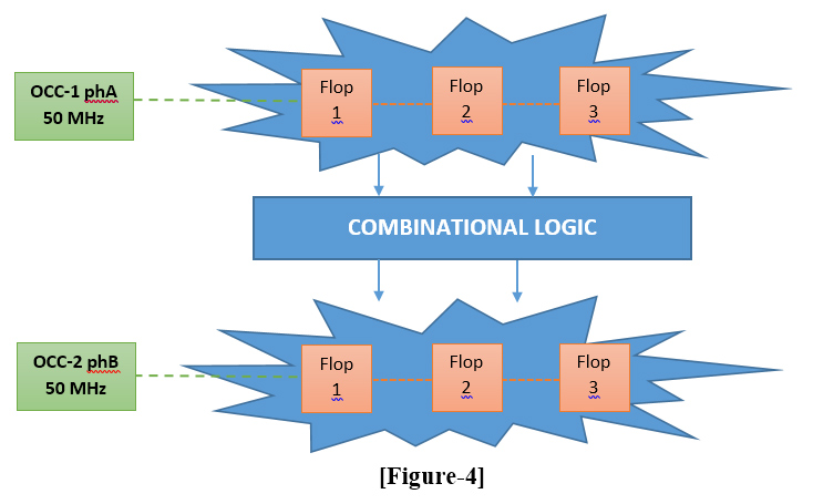
To overcome the hold violations in SA-capture mode, the approach is to perform launch and capture from two phase-shifted clocks with a specific delay. We can insert two OCC’s (On-chip clock controller) in design for two phases of the same clock-domain. This means, for a single clock-domain there are two OCC’s inserted as shown in Figure-4 below. An OCC can be programmed to generate a single pulse only. Now, to test the combinational logic between them, the approach is to launch from PhA and capture from PhB, and vice versa.
Here, the goal is to cover the stuck-at faults between two phase-shifted clocks. Hence, the slow frequency will be used for capture from OCC. Instead of doing static ATPG we will use dynamic ATPG. This can be achieved by generating a single launch pulse from OCC-1 and after some delay generating capture pulse from OCC-2. This way PhB clock can get enough time to hold the data.

Here, only the phase of clock changes for each OCC and the frequency remains the same for all OCCs. That means, if you have four phase-shifted functional domains of 500MHz, then you will need four OCCs. However this method increases the small amount of area, it helps cover the faults between phase-shifted domains.
DOWNLOAD CASE STUDY
Design for Testability for a High-speed Gigabit Ethernet Controller for Networking
The On-chip-clock-controller (OCC) from various EDA vendors, supports the programming of delay-counter registers. This helps to modify the delay of capture pulse coming out of OCC after SE is low. We can set the delay in such-a-way that PhA-OCC1 generates launch pulse and PhB-OCC2 generates Capture pulse and vice-versa. This way, we will be able to cover Stuck-at faults between PhA and PhB.
Figure-5 shows how both the OCCs generate capture pulses in scan-mode when SE is low to detect Stuck-at faults.

Conclusion:
In mixed signal-processing circuits where the design uses phase-shifters and the design complexity is high, it is difficult to fix timing (hold violations) for stuck-at capture mode. By the method mentioned in this article, we can test the logic between phase-shifted domains without fixing hold violations.
With a proven physical design flow, methodologies, and with dedicated subject matter experts, eInfochips has provides RTL to GDSII services many clients for successful Silicon tapeouts. Know more about our Physical Design and DFT Services.


