Executive Summary
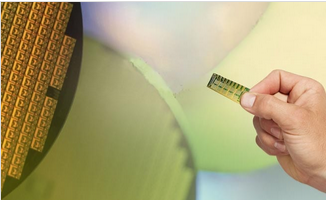
Client is a leading industry player in complex ASIC solutions with significant time-to-market and performance advantages in high-speed computing, networking and storage applications. There was a requirement to enable SDN (Software Defined Network) functionality within this chip. Given the size and logical complexities, the client had no option but to choose 16nm technology node.
Having delivered multiple projects for the client, eInfochips was chosen to work on its first 16nm FinFET program based on capabilities and quality checklists. TSMC’s 16nm FinFET program allows unprecedented power efficiency and form factor advantages to the chip. Given that it is designed for 24×7 operational SDN routers, it would significantly bring down the power consumption for the product, and operational expenses for end users.
The client taped-out the first (of three variants) of the 16nm chips in early 2015, which has been subsequently deployed by a Fortune 100 company.
Project Highlights
- 16nm Node for TSMC Tape-out
- 96 Tbps NW Data-rate Support
- Over 1 Billion Logic Gates
- 25mm X 28mm Die Size
- 1 GHz Operating Frequency