The recent increase in the technology usage and the competition to acquire global market has cornered the industry to move into lower Technological nodes with higher increase in Transistor’s per die, thus creating new challenges in ASIC manufacture testing. To counter this and achieve higher testability in a SoC device, various DFT structures are inserted in the design, such as memory BIST, scan, boundary scan to name a few, this is resulting in increasing ASIC design factors like power consumption during test mode, over-all area of the chip and tester time along with coverage, day by day. The purpose of this article is to highlight the different methodologies to reduce power consumption during ASIC manufacture testing. It distinguishes the different architectures & methodologies to optimize power consumption during a test mode of the design with implementation. There are number of techniques to reduce power consumption with different EDA tools available in the industry. This article explains a few “power-aware” techniques, discusses and compares between few software-based & Hardware based implementation method with one of the “Synopsys EDA tool” taken as a case study.
I. INTRODUCTION
As we move towards the lower technology nodes (165nm-> 130nm-> 90nm-> 65nm-> 28nm-> 20nm-> 16nm-> 10nm-> 7nm-> 5nm), transistor per unit area is being increased which is resulting in rising the amount of current consumption per unit area causing more dynamic switching and leakages. This has forced the design teams to leverage a number of power-related strategies as shown in the figure.
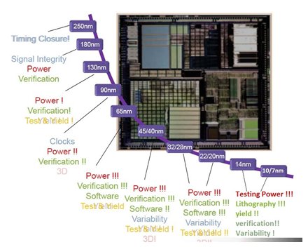
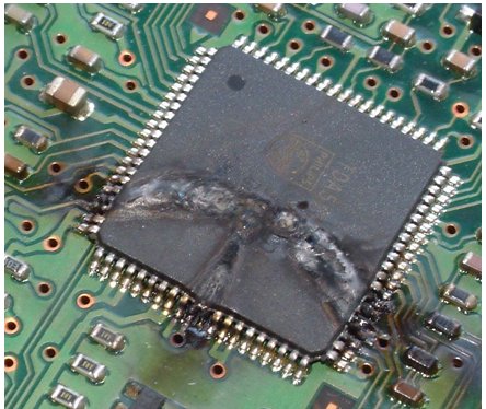
As die density increases, power dissipation during scan-based tests is higher than the functional mode this is because efficient test patterns cause a very high percentage of the logic being switched at a given time [3] resulting in higher stress during test mode. It creates the possibilities of chip failure on tester as some chips would melt unless different blocks are shut down at different times which ultimately results in higher tester time.
In addition, current leakage begins increasing which results in heat dissipation, as transistors are physically dense to each other these heats are trapped between the fins. These effects can also lead to degradation of the chips as a result of various thermal effects. This might also lead to reliability loss of a device as a result of conductors being exposed to intensive erosion. As such, understanding such a negative factor and finding a suitable remedy is equally important.
II. DIFFERENT METHODOLOGIES FOR TEST POWER OPTIMIZATION
There are many Techniques proposed, tested and Implemented to some extent across industries in order to reduce the power loss during shift transition in test mode. Implementing this to the live projects are of a bigger challenge as even the original design requirements along with area overhead and tester time will be in high consideration. Broadly these methods can be categorized as Hardware-based and ATPG based (Software based).
Hardware-based targets power reduction technique applicable during Scan Insertion and Software-based during pattern generation. Existing SCAN/Hardware-based solutions require either to partition the scan chain architecture and test one partition at a time or insert additional hardware into the design. The partition-based architecture is achieved by splitting unit scan segments into multiple segments. So that only a specific number of scan segments can be enabled at a time.
The better way of splitting is achieved through length wise splitting for keeping scan shift cycles same across all scan segment. By use of external controlling gates, unnecessary scan chain transition can be prevented by propagating into the circuits. Due to this, performance degradation can be observed, as it impacts on critical path delays [7]. Thus ultimately these techniques crackdown to compromising in any one of the 3 main design perks (Area, Power & tester time) reducing power ultimately leads to either increase in Area size or increase in Tester time. The designers need to decide which aspects to be compromised and prioritized.
Below lists a few techniques in which power optimization is achieved but by compromising either Area or Time.
A. SCAN/Hardware-based
Shift Power Groups technique: One method used widely across the industries is the use of Shift Power Groups technique. This technique is used to reduce power consumption during scan Insertion methodology. It is achieved by inserting AND gates at the decompressor outputs before each compressed scan chain. The chains are gated in groups that are controlled by a shift power control (SPC) [4] chain, as shown in the figure below.
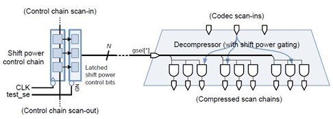
The SPC control groups are special control signal groups active only during the shift period of the active test mode duration. These controls enable during compression based scan testing which is built during Scan Insertion. Even though these are applied after the decompressor block and before scan chain, it does not form a part of scan chain or Compression logic. Instead, it is an external (uncompressed) chain outside the codec logic.
The SPC contains register chain, containing group mask values for the next patterns. Thus by predicting the present and next pattern shadow latches retain the bits present in the mask values for the scan-in of the next pattern. Masked groups load constant values into their chains, which reduces overall toggle activity. The SPC chain again can-not be a part of compression chain as compressing it would lead to gating itself thus preventing it from loading any reliable pattern.
Functional output gating technique: Even during the scan shift phase of DFT-scan test, the patterns loaded will trigger the functional path and cause toggling for every shift thus causing functional logic to be in always active state even while not in capture mode [1]. This can result in huge dynamic power loss and caused unnecessary power consumption.
As described above in the introduction part, an increase in power consumption may affect chip quality in terms of yield. It may damage the whole chip. By using Functional output gating suppression technique, different EDA tools can help to modify a design structure or designer can modify by their own in such a way that it can control the toggling activity in scan insertion. One normal way to do it is by implementing AND- gating or OR-gating logic, depending on which constant value most reduces toggling from other ungated signals entering the fan-out logic cone.
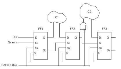
As shown in the image below an AND gate is inserted between Scan flop out (SOUT) and Functional IN. The control to this can be achieved by using already existing signal Scan Enable (SE) thus while in shift mode functional path will be gated OFF and while in Capture mode the gate allows the flow of required pattern into the functional logic.
The SE signal acts as a control signal for switching since during Shift mode it will be high and during Capture mode, it will be low thus automatically allowing for the switching action of the Functional gating logic.
This method uses only a small amount of additional area overhead and is one of the best method implemented throughout industries. Saying that it does not mean this method is free of any shortcomings and challenges, one major consideration needs to be taken care for this is during the implementation of Transition fault model testing.
Primary reason being, it introduces extra gate delay in functional path thus timing closure is to be done for this gate too considering it to be in the functional path. Secondly, LOS method of transition has a large disadvantage as the last shift of the pattern acts as Launch pulse and is followed through the functional path, but if the Functional gating is in inactive state then no proper test bits are loaded this might happen because during last shift i.e. launch phase Scan Enable will be High resulting in driving the functional gate to act in inactive mode. So extra logic again will be required to solve this, ultimately resulting in taking up even more space.
Scan chain modification technique: In order to achieve parallelism in testing with lower peak-test power, Scan chain modification technique [9] incorporates this by slightly modifying the scan chain based on the analysis of pre-generated test set. Here reduction in test power can achieve with inserting logic gates between the scan FF’s. As these insertions of logic gates are only in the scan path, no gate delays are induced to the critical or functional path. Thus guaranteeing no interference with the normal operation too.
The insertion of logical gates in scan chain depend on the analysis result. But this insertion should be bijective, it must be taken care so that these test sets do not produce any dependencies on test data. The insertion should be in such a way that it should result in no controlling value and the mapping of test vectors should be discrete to stimuli. An example for this method is explained as below: An inverter, between two scan cells, necessitates the transformation of the actual test data that passes through this gate; it is to be taken care that no changes between, original and negated data bits passing through an inverter, be observed. The transition between only these two bits is negated and is expected as such, and should not affect any other transition. As such it can be considered that this modification is a transition-preserving one with only test data bits having a local impact.
The analysis is done by decomposing the test data into blocks of 3 bits and transitions power estimate is calculated for all 8 combinations formed from these 3-bits, then the modification with minimum transition is implemented to the corresponding scan chain fragment.
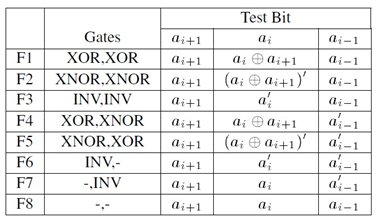
This method ensures with higher test power reduction with a little area overhead. Since in order to implement it for maximum use, all the scan chain fragment are to be analyzed and experimented to attain ideal scan chain modification. Due to which this method can be implemented for a design with lower scan chain fragment and implementing it for design with huge scan chain element results in extended DFT implementation time which might not be ideal in most cases.
Freezing Power-Sensitive RTL Bits: Freezing Power- Sensitive RTL Bits is a method to reduce switching activity by stagnating small segments of all FF’s at RTL Level. Even with lower area overhead, switching activity can be reduced greatly. [8]. Design’s budget is directly proportional in deciding the freezing bits. In comparison with other methods, which freeze these FF’s at the gate level, timing closure can be more easily met. At the gate level, STA timing analysis needs to be taken care well to check that the FF’s timing not affected by freezing methodology. Also at RTL level, we can allow synthesis tool to fix the timing and the close it at the back end.
B. ATPG/Software Based Technique:
Primary input freezing technique: One of the power-aware technique during test vector generation is to freeze the primary input part which can reduce contrived transitions during test application to save the total amount of transitions occurred [6]. The output capacitance will charge/discharge by dynamic power for every gate which is as below;

Where load capacitance named as Cload, VDD is the supply voltage, Tcyc is the global clock period, and NG is the total number of gate output transitions (0 -> 1 or 1 -> 0). As per the equation; the major reduction in power will be because of, decreasing few variables in the above power dissipation (Pd) equations. An invalid transition during test application is a transition which occurs in the combinational part of the circuit under test while shifting out the test response and shifting in the next test vector. (Also it is not having any impact on test efficiency since there is no useful data impacting on test efficiency at output & input. Furthermore, the value of primary inputs is irrelevant during shifting out the test response.
Shift power budget technique: One of the Software based ATPG technique is a power-aware methodology. Here fanout of all clock-gating structured are calculated and test vectors are created taking this result into account. This techniques [2] are well implemented across all modern-day EDA tool vendors. In one such tool (Synopsys) flow, the calculation of clock-gating structures is done in the DRC stage which then helps in generating test patterns by setting capture and shift power budget in terms of percentage. It controls the toggling activity in the design by taking power effort and budget as per the design criteria.
Power-constraint-scheduling-of-tests: One most easy way to implement and widely used technique for test power reduction is “test scheduling” method. Its advantage suffices by meeting 2 purposes i.e. reduce test power and also manage the resource. This technique [5] was mainly implemented taking resource into consideration, as in most cases not all the test can be applied at once, take for example an SoC with multi L2 L3 level blocks but with only 8 10 top-level scan ports, it might not be able to run test on all blocks at a single given instance. Hence scheduling of test for few blocks at a time gives resource management advantages as well as automatically reduces the power consumption stress of SoC. during testing.
The method “power-constraint-scheduling-of-tests” [D] uses this scheduling of tests in a much more structural way, by developing an algorithm to group the similar test cases and schedule it together for higher power reduction during testing. This method is archived by mainly following 3 steps. First is to find a complete set of time compatible tests with power dissipation information associated with each test.
Then using these tests, a list containing power compatible tests are extracted. And finally, a minimum cover table approach to find the optimal scheduling of the tests is used. As advantage suffices it doesn’t mean it is free from other negative effects. One main design aspects that take a deleterious effect is tester time. More the scheduling more the time need for testing.
III. IMPLEMENTATION STATISTICS
A. Hardware-Based Statistics
This hardware-based statistics covers one of the scan chain modification technique implementation as described in introduction part. It contains detail analysis reports in terms of three main factors such as area, power and test coverage which affects test methodology.
1) Area Statistics

2) Power Consumption Statistics

3) Test Coverage Statistics
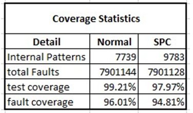
B. Software Based Statistics
We have performed a case study on one of the EDA vendor’s ATPG based power-aware techniques to reduce toggling activity during the scan and compare its actual behaviour including different statistics as shown in below figure 9. It contains 2 main factors, which is affected by using this methodology. As it is one of a software-based technique, the physical area is not affected.
1) Power Consumption overall statistics
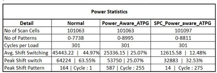
2) Test coverage statistics

IV. CONCLUSION
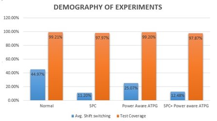
From the analysis, we conclude one of the most affected parameters during DFT is shift power consumption on lower technology nodes. As we can see in the below chart, how different techniques lead to a decrease in power consumption with some parameters drawback as a small decrease in test coverage and little area overhead. Also, we can say that fault caused by a timing or power issue during scan testing might never occur during the functional mode of operation and would introduce unnecessary yield loss, this is a big concern for the industry. This paper includes both Hardware and Software based techniques with detail statistics.

REFERENCES
[3] https://www.design-reuse.com/articles/32262/low-power-design-for-testability.html.
[4] Reducing power consumption in dftmax ultra designs.
[5] Richard M Chou, Kewal K Saluja, and Vishwani D Agrawal. Power constraint scheduling of tests. In VLSI Design, 1994, Proceedings of the Seventh International Conference on, pages 271–274. IEEE, 1994.
[6] V Dabholkar, S Chakravarty, I Pomeranz, and SM Reddy. Techniques for reducing power dissipation during test application in full scan circuits. IEEE Transactions on CAD, 17(12):1325–1333, 1998.
[7] Stefan Gerstendörfer and Hans-Joachim Wunderlich. Minimized power consumption for scan-based bist. Journal of Electronic Testing, 16(3):203–212, 2000.
[8] P Giribabu and G Sunil. Dft-based approach for reducing switching activity during scan shift.
[9] Ozgur Sinanoglu, Ismet Bayraktaroglu, and Alex Orailoglu. Test power reduction through minimization of scan chain transitions. In VLSI Test Symposium, 2002. (VTS 2002). Proceedings 20th IEEE, pages 166–171. IEEE, 2002.
Saumil Modi, Janki Chauhan & Sanketh Aipanjiguly

