Executive Summary
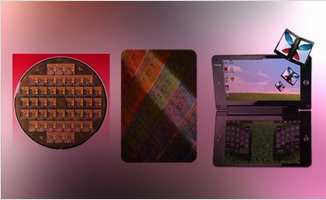
This low power mobile SoC is targeted for next generation mobile devices. The evolution of mobile devices into multi-feature smartphones has put stringent requirements on perfromance and power consumption of the chips that goes into such devices. To address this challenge, the client planned to introduce a chip that supports multiple power domains and Voltage Frequency (VFS) Scaling to optimize power consumption. This multi clock domain design chip had total 16 Power Domains, 6 shut off & 8 DVFS and operated at 1.1 core voltage.
The customer partnered with eInfochips based on proven track record of successfully managing complex RTL to GDSII implementation projects involving advanced process technology nodes and low power design techniques. In addition, eInfochips also offered Design for Testability (DFT) services for the chip.
Project Highlights
-
- Toshiba 40nm Technology Node
- Total 16 Power Domains, 8 DVFS
- Highest clock frequency 780MHz
- Functionality: 2G, 3G, LTE, CDMA,
- GSM, Base band Modem, Core Signal Processors